Cloud storage supplier Wasabi is a stick-to-your-core-focus business and its core focus is offering disk drive-based S3 object storage in its cloud, with the pitch being that it’s cheaper than Amazon with no egress fees.
Update: Note on Backblaze reserve capacity deals added. 29 November 2023.
Jonathan Howes
Although Wasabi is not a technology trailblazer it must be doing something right because, as EMEA VP Jonathan Howes pointed out, Wasabi is growing at twice the cloud storage market’s average growth rate, according to IDC numbers. In late 2022 it had more than 40,000 customers and Howes says it now has 60,000.
Howes and Wasabi’s VP for Cloud Strategy, David Boland, briefed us earlier this month and extended what we had learnt from an interview with Wasabi CEO and co-founder David Friend in February. Boland said Wasabi basically replicates its cloud datacenter pattern in each of its 13 regions. A set of servers and disk-based storage chassis plus software will be installed in a co-location datacenter, often one run by Equinix. It’s expanding by growing the customer base in a region and also by adding regions.
There is no wish to add additional tiers of storage, such as, for example, a tape archive tier, or faster-access SSD tier. It does supply a file access service, Wasabi Cloud NAS, but this is basically a NAS gateway running on-premises and providing file-access to files stored as objects in Wasabi’s S3 cloud repository.
It also supplies multi-tenancy and accounting software to its MSP customers so they can sell white label or Wasabi-branded cloud storage to their customers and get up and running in a short time.
David Boland
Howes said Wasabi has qualified its software as a backup target for data protection suppliers, such as Veeam. He claimed that it’s not seeing competition from on-premises, object-based backup targets, and suggested these serve a separate market. Nor is Wasabi seeing competition from Web3, decentralized storage suppliers, it told us.
Howes agreed that Wasabi is a tier 2 cloud storage provider, in general revenue terms, with AWS, Microsoft and GCP in tier 1, and CSPs such as Backblaze and OVH Cloud in a tier3.
Wasabi charges $6.99 per TB per month pay-as-you-go storage while Backblaze charges $6.00 per TB per month, with neither charging egress fees. However Backblaze does levy an egress fee of $0.01/GB once a customer downloads more than three times the average monthly data stored amount.
Backblaze pricing.
Even though Backblaze has an upfront pay-as-you-go pricing advantage, Wasabi says it can undercut it by selling reserved capacity storage with 1, 3 and 5-year terms, giving customers substantial pricing discounts for capacity purchase commitments on this basis. Backblaze also offers reserve capacity pricing deals. Wasabi says it covers more geographic territories than Backblaze.
Howes says customers find egress charges objectionable. While allowing that Wasabi operates under an AWS/Azure and GCP price umbrella, he doesn’t think think that the big three will lower their egress prices – because they make too much money from it, and also because Wasabi and its competitors are not hurting the big three enough.
S3 cloud storage is fertile ground. Howes says Wasabi can stick tightly to its S3 knitting and continue to grow for the foreseeable future.
Startup Iridia is combining semiconductor, enzymology, and microfluidic biochemical techniques with the aim of producing a read-write DNA microchip with archival storage capacity.
The company reckons that DNA storage is essential due to the enormous and ever-growing amounts of data requiring archival, which incurs significant costs in terms of money and electricity. DNA storage has the promise of revolutionizing archival storage because it is highly stable, has many orders of magnitude more capacity than tape cartridges, and will need far less electricity to operate.
James Linton
Timeline
2015 – founded as Dodo Omnidata by director and CEO James Linton and others
2017 – $400K seed round. Investor Jay Flatley joins board
2018 – $2.1 million A-round
2019 – Murali Prahalad becomes CEO and president
2021 March – $24 million B-round funding, with investors including Western Digital
2021 December – $6 million equity fund raise
2022 March – Trey Cauley hired as VP Engineering
2023 July – Buck Watia hired as VP Corporate Development to chase strategic alliances
Iridia’s chairman is Jay Flatley, who also chairs the board of DNA sequencing company Illumina, where he was CEO from 1999 to 2016.
Technology
Iridia wants to build a DNA memory chip and practical DNA storage mechanism with its technologies. A 134-page patent filed by CTO and head of research Paul Predki in September 2017 provides an indication of what it’s doing.
The technology involves nanopore-based cells with data (DNA strands) moved inside the cell, and data written (DNA strands added) and read (DNA strands sequenced) with error checking and correction. The chip will contain reservoirs filled with reagents, with fluid moved through tubes and into and out of reservoirs by commands from the semiconductor (CMOS) part of the chip. Individual elements have been proved to work and the bulk task now is integrating them on a single chip.
A nanopore is an electro-resistant membrane or flow cell embedded with nano-sized holes and electrodes hooked up to sensors. It is placed between two reaction compartments. The sensors measure electric current flowing through the nanopore and its capacitive variance disruption as molecules of DNA pass through the pores. An analysis of the disruption patterns reveals which of the four oligonucleotide DNA bases – A, T, G and C – has passed through, i.e. the DNA is sequenced. Only two base types are needed to indicate a binary one or zero so either A and T could indicate zero and G or C a binary one.
Reaction compartments and nanopores can be used to build DNA sequences (writing) and separate compartments to read (sequence) the DNA patterns. In this Iridia approach, the DNA memory chip carries out writing and reading.
The patent describes an existing DNA storage approach, in which data is encoded in blocks. For example, one bit per nucleotide, with 96 data bits and a 19 address bits per block. When read (sequenced), the data blocks are arranged in the correct order using the address bits, and the sequence data converted to binary code. Iridia’s patent talks about its new approach supporting DNA strands that are hundreds, thousands or millions of bases (bits) long. A nanopore reader can read up to 1 million bases per second.
Capacity and speed
Iridia claims that 1 gram of DNA contains the same amount of data as 10 billion 6 TB disk drives, meaning 60 billion terabytes, 60 million petabytes, or 60,000 exabytes.
Murali Prahalad.
CEO Murali Prahalad said in an interview that the product being developed by Iridia will have much lower read and write latency than tape, 2,500x lower power consumption than an SSD, and reduce exabyte-class datacenter costs by up to 99 percent if Iridia’s chip was used to store archive data. These are attractive numbers if accurate.
He talked about Iridia’s chip having theoretically four orders of magnitude more capacity than tape or hard disk drives. Based on 18 TB raw capacity from an LTO-9 tape, that would mean 10 x 10 x 10 x 10 = 180,000 TB (180 PB). Based on a 22 TB disk drive, it would mean 220 PB.
Although Prahalad discussed a DNA memory chip, he also mentioned a physical device having the footprint of a 3.5-inch disk drive or tape cartridge that would contain several DNA memory chips. Supposing five of them are contained in the device, we are looking at about a petabyte of capacity. If this can be realized with an affordable price and acceptable performance and endurance, Iridia’s technology would surely have merit.
Progress
The $24 million from the 2021 B-round was intended to help pay for Iridia to double its headcount from 10 to 20. The $6 million follow-on was to be used for further validation of Iridia’s technology and the development of working prototypes.
Trey Cauley’s hire is involved with prototyping Iridia’s technology while Watia is working to build strategic alliances to help bring it a product to market.
The next major milestone will be the production of a prototype DNA memory chip and checking out its capacity, performance, and endurance for further development.
It seems to us that DNA memory chips means you need a computer system to hold the index of information on them, a chassis in which to store the DNA memory cartridges, plus software to control the writing and reading of data by the DNA memory chips inside the cartridges. You won’t need robotics to bring the cartridges to read/write drives as the chips in each cartridge read and write data as well as store it, like SSDs.
A chassis could be filled with empty DNA memory cartridges and, as their capacity is used up over time, they could be augmented with additional chassis. Although DNA can last for thousands of years, a DNA memory chip with onboard fluid tanks may deplete over time, potentially affecting functionality.
Seagate is also developing lab-on-a-chip technology for DNA storage in partnership with DNA storage startup Catalog Technology.
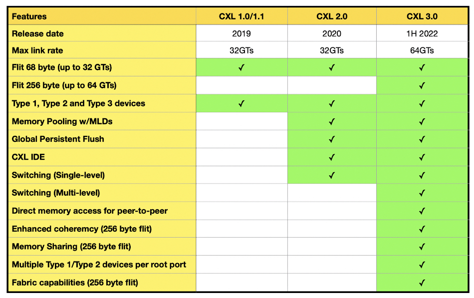
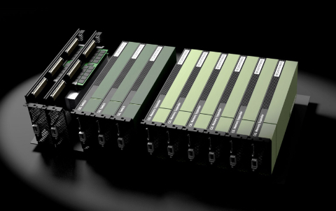
Korean technology firm Panmnesia has a CXL 3.0-enabled accelerator chip which provides sharable memory to speed AI applications.
CXL (Computer eXpress Link) 3.0 enables a pool of external memory, accessed through CXL switches, to be shared between host computers with coherent caches in the hosts and the CXL memory endpoints or expanders. The earlier CXL 2.0 standard enabled hosts to access their part of an external memory pool via a CXL switch but not share it. The initial CXL 1.0/1.1 standards supported a host having direct access to external memory without going through a switch.
The forthcoming CES 2024 show has given Panmnesia an Innovation Award for its accelerator chip.
Panmnesia founder and CEO Myoungsoo Jung said in a statement: “We believe that our CXL technology will be a cornerstone for next-generation AI acceleration system. We remain committed to our endeavor revolutionizing not only for AI acceleration system, but also other general-purpose environments such as data centers, cloud computing, and high-performance computing.”
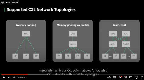
The company contrasts its ability to provide up to a theoretical 4PB of shared memory with clustered servers accessing external SSDs for data. It says that individual servers generally work in parallel on AI and other HPC-style applications and need to access more data than can be held in their memory. That means they have to use SSDs to store the excess data and access them by SAS, NVMe or RDMA protocols across a network.
It is better – faster – to load all the data into an external memory pool and have all the servers access it using memory load and store instructions with data crossing a PCIe 6 bus instead of a slower network link.
The accelerator chip is part of a Panmnesia All-in-One Framework to help developers build proof-of-concept CXL 3.0 system software, user-level applications and custom hardware. It includes the accelerator chip which has a built-in CXL 3.0 controller, CXL switching and end-points. These are are fully compatible with all CXL protocols, such as CXL.io, CXL.cache, and CXL.mem.
The switch has a software fabric manager function to manage internal routing rules within the switch, and can connect to other CXL switches and external devices,
The framework justifies its All-In-One name by having a software stack featuring a Linux-based OS with CXL device drivers and a CXL-aware virtual memory system. This means applications can use the shared CXL external memory with no code change
Panmnesia’s memory sharing uses back invalidation to enable endpoints, the memory expander modules, to manage the cache coherency between hosts. There is register-to-register transfer between a host and its accelerator chip.
A You Tube demo video shows 8TB of CXL-attached memory being made available to the host and 8KB of the memory space set shareable. Another host could then access the sharable memory and the two hosts share data via the shared memory space.
Panmnesia says that some HPC plasma simulation applications speed up 1.8x by using its shared memory instead of accessing SSDs to get data. It also claims that AI applications can achieve an up to 101x speed up through the accelerator chip, because it is tailored to AI search with frequent parallelized vector processing.
CES 2024 will take place in Las Vegas from January 9 to January 12.
Panmnesia raised a $12.5 million seed round in September, giving the company an $81.4 million valuation. The round was led by Daekyo Investment, with participation from SL Investment, Smilegate Investment, GNTech Venture Capital, Time Works Investment, Yuanta Investment and Quantum Ventures Korea.
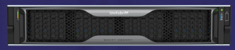
UnifabriX MAX.
Israeli startup UnifabriX is also working in the CXL 3.0 shared memory area with its MAX memory and storage machine. It has an Early Access Program (EAP), with agreements with High-Performance Computing (HPC) entities for MAX testing and validation. This has been expanded to include companies with on-prem/cloud data centers needing to handle AI workloads.
AvePoint has announced the launch of AvePoint Cloud Backup Express, which, running on Microsoft 365 Backup Storage, enables customers to protect and secure their SharePoint, OneDrive, and Exchange environments. It keeps all data within the Microsoft 365 security boundary.
…
Data lakehouse supplier Databricks has integrated technology from generative AI supplier MosaicML – which it bought in June for $1.3 billion – into its own offering to produce a Data Intelligence Platform on top of its lakehouse. It enables customers to create an internal “AI factory” where they can train and deploy models on private data at an accessible cost.
MosaicML now offers multiple capabilities to directly integrate enterprise data into AI systems including:
End-to-end RAG (Retrieval Augmented Generation) to build high quality conversational agents on your custom data, using Databricks Vector Database for “memory”
Training custom models either from scratch on an organization’s data or by continued pre-training of existing models such as MPT and Llama 2 to further enhance AI applications with deep understanding of a target domain
Efficient and secure serverless inference on your enterprise data, and connected into Unity Catalog’s governance and quality monitoring functionality
End-to-end MLOps based on the popular MLflow open source project, with all produced data automatically actionable, tracked, and monitorable in the lakehouse
Astra DB Database-as-a-Service (DBaaS) supplier DataStax has introduced Astra DB Assistants API, which is a drop-in replacement for the OpenAI Assistants API. OpenAI Assistants API handles all the stateful operations required for large language model-based applications including persistent threads and messages, files, and automatic RAG. Astra says the end result is a simple, scalable datastore for AI apps that’s backed by the power of Cassandra. It is available as a developer preview. Read a blog about it here.
…
DDN has joined the Vultr Cloud Alliance. By integrating DDN’s data management systems with Vultr’s composable cloud infrastructure, data science and engineering teams will gain optimized data operations, migration, and protection for their AI initiatives across Vultr’s global network of 32 cloud datacenter locations. Vultr says it’s the world’s largest privately held cloud computing platform, and offers Cloud GPU (Nvidia), Cloud Compute (VMs), optimized Cloud Compute (NVMe SSDs and VMs), and Bare Metal servers.
…
HPC storage performance watcher Glenn Lockwood writes of DDN’s new Infinia file system software: “The engineering team developing Infinia inside DDN is completely separate from the Whamcloud team who is developing Lustre, but this could be a double-edged sword. On the good side, it means that open-source Lustre development effort isn’t competing with DDN’s proprietary product in engineering priorities on a day-to-day basis. On the bad side though, I still struggle to see how Infinia and Lustre can avoid eventually competing for the same business.
“For the time being, Infinia does seem to prioritize more enterprisey features like multi-tenancy and hands-free operation while Lustre is squarely aimed at delivering maximum performance to a broadening range of workloads. Their paths may eventually cross, but that day is probably a long way off, and Lustre has the benefit of being deeply entrenched across the HPC industry.”
…
Fantom Drives has released its VENOMX SSD for gaming, virtual reality, and video production. There are 1 TB and 2 TB models in the M.2 format, supporting PCIe gen 4 and an NVMe interface. Read/write speeds reach up to 5,100/2,600 MBps. The drive’s feature set includes dynamic caching, TRIM support, SMART (Self-Monitoring, Analysis, and Reporting Technology), APST, LDPC ECC algorithm, end-to-end data path protection, and AES 256-bit encryption. They have up To 1500 TBW endurance and 1.5 million hours of MTBF, and a five-year warranty.
Mark Cree
…
Unstructured data orchestrator Hammerspace has hired former AWS GM Mark Cree as SVP of Strategic Partnerships. Cree ran AWS’s storage gateway business. Before that he was CEO and founder of InfiniteIO, which used metadata acceleration to speed file access, not a million miles from what Hammerspace does now.
…
Infinidat said Japanese commercial online karaoke supplier XING consolidated its enterprise storage on the InfiniBox platform five years ago, simplifying its infrastructure (27 storage systems from four different suppliers). As a result, we’re told it improved performance, saved space, and achieved an annual cost saving of 80 percent by substantially reducing the equipment and maintenance costs associated with the previous storage devices, and with no downtime since then. Read a case study here.
…
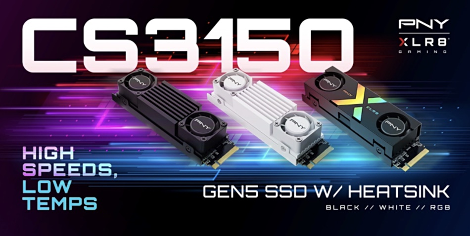
PNY has a CS3150 PCIe gen 5 gaming SSD in M.2 2280 format, operating with up to 12,000 MB/s and 11,000 MB/s sequential read/write speeds, available in 1 TB and 2 TB densities, and comes with dual-fan heatsinks. It uses Microsoft DirectStorage, which was introduced in Windows 11 and improves the speed at which games load and the quality of their images. TCG Opal 2.0 is enabled for hardware encryption and storage security – an odd feature for a gamer’s SSD. The drive has five-year limited warranty and is priced at £165-£175 for 1 TB.
…
Proton has announced its Proton Drive app for macOS which provides encrypted public cloud storage. The app lets you sync files between your Mac and the cloud, access them offline, free up space on your computer, and has end-to-end encryption. Proton says it already supplies Proton Drive apps for iPhone, Android, Windows, and the web. It’s a Dropbox competitor.
…
Real-time analytics platform Rockset has expanded its vector search capabilities with approximate nearest neighbor (ANN), achieving billion-scale similarity search in the cloud. This comes after Rockset raised $44 million in funding in August, and was named a data streaming for AI partner to Confluent.
…
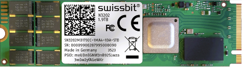
Swissbit has an N3202 high-performance PCIe gen 4 SSD in an M.2 2280 form factor using TLC NAND. It has a DRAM-based controller architecture with endurance of up to 1.5 DWPD over a five-year period. The N3202 is available in 240 GB, 480 GB, 960 GB, and 1920 GB capacities.
…
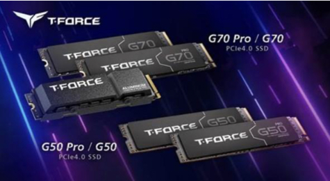
Team Group has released four new T-FORCE PCIe gen 4×4 SSDs: the G70, G70 PRO, G50, and G50 PRO drives, all using InnoGrit’s controller. They are available in the M.2 2280 form factor and come with thin graphene heat sinks. The G70 and G70 PRO SSDs have read speeds of up to 7,000 MBps, while the G50 and G50 PRO SSDs can clock up to 5,000 MBps. The G70 and G50 SSDs support SLC cache technology, and their PRO variants support both DRAM and SLC caching.
…
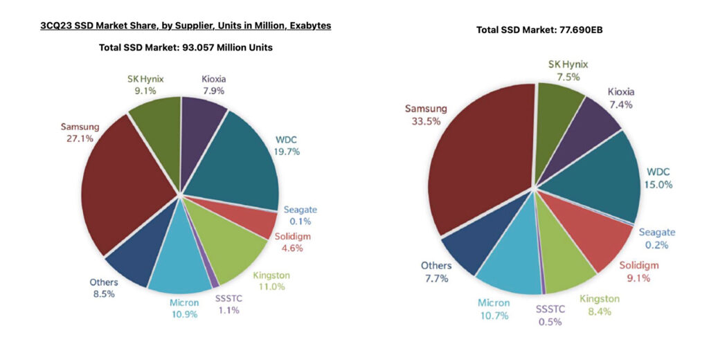
Thanks to Storage Newsletter, we got to see TrendForce stats for Q3 2023 SSD units and capacity sales by supplier, with both PC SSD and enterprise SAS SSD sales pushing up the numbers. Unit shipments were 93.06 million, 24 percent higher Q/Q, with client SSD units rising 27 percent and enterprise PCIe SSD units going up 34 percent to 3.77 million ships. The increased client ships helped overall NAND bits to rise 6 percent to 205.35 EB. SAS SSD units grew 26 percent Q/Q, reaching 0.702 million, while enterprise SATA SSDs dropped 5 percent to 3.34 million, with SAS SSDs squeezed between NVMe and SATA. The supplier units and capacity shipped shares were:
In unit terms Samsung is the clear leader, with Western Digital in second place followed by Kingston, which is not a NAND manufacturer, and then Micron, which is in fourth place. If SK hynix and its subsidiary Solidigm’s shares are combined, they would have 13.7 percent, putting them in third place. Were we to combine Kioxia and NAND foundry joint venture partner Western Digital’s shares, we get 27.6 percent, putting the pair ahead of Samsung in unit shipments.
Doing the same calculation with capacity shipment shares puts the duo at 22.4 percent, well behind Samsung’s leading 33.5 percent share. Combining SK hynix and Solidigm capacities produces a 16.6 percent share, putting them in second place ahead of Western Digital on its own at 15 percent.
Richard Wainwright
…
Data protector/manager Veritas has hired Richard Wainwright as field CTO for UK and Ireland to lead a team of technical specialists and be responsible for technology strategy and solution architecture. Wainwright joins Veritas from fintech startup R3, where he led the development of a SaaS platform for Corda, a distributed ledger technology. His CV includes stints at Tectrade, Dimension Data, Nortel, and Avaya. Veritas also released market research that shows that nearly half of all global organizations may be miscalculating the severity of threats to their business.
…
ReRAM startup Weebit Nano says it has received the first wafers integrating its embedded ReRAM manufactured in GlobalFoundries’ 22FDX platform. Initial tests of the wafers in this advanced 22 nm FD-SOI (fully depleted silicon on insulator) are showing positive results on the array. Weebit says 22 nm is a geometry where embedded flash is not viable.
…
Weebit and SkyWater announced that Weebit’s ReRAM IP module has been fully qualified in SkyWater’s S130 process at temperatures of up to 125°C – the temperature specified for Grade-1 automotive applications.
Belgium-based Nodeum is a 10-person outfit with its file management software used by 30 customers, including five of the top European high-performance computing centers. How did such a small company achieve this level of influence?
Its software is used to manage the storage of file data, moving it from primary through to secondary (disk) and tertiary (cloud, tape) storage – classic hierarchical file storage lifecycle management in other words. This is an area with well-known suppliers such as Komprise, SpectraLogic (StorCycle), Atempo (Miria), and Quantum (StorNext), yet Nodeum has built up a customer base despite heavyweight competition.
Valéry Guilleaume
CEO and co-founder Valéry Guilleaume said Nodeum was indeed a small company, with annual revenues around €1 million ($1.1 million).
HPC customers include the Jülich Supercomputing Centre, Barcelona Supercomputing Centre, and the CSCS Swiss National Supercomputing Centre, plus Fenix and its confederation of six European HPC sites in the Human Brain Project research initiative.
They have taken on board Nodeum’s concept of a three-tier archive – immediate access, intermediate access, and a long-term archive pool.
The company was founded in 2015, and launched its first product in 2016. The initial customer in the Germany-Austria-Switzerland (DACH) region was won in 2020, which was also when a UK distribution agreement was set up.
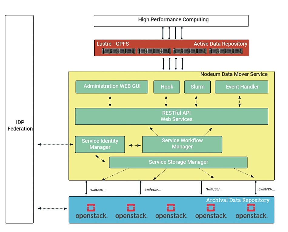
Nodeum has no formal go-to-market organization, being mostly engineers who have built a large-scale, POSIX-compliant file system with dataset retention, metadata, indexation, and data movement capabilities. This system can work with an HPC site’s Lustre and GPFS parallel file system software, and Nodeum understands HPC workflows and use of multiple different file and tape storage supplier’s systems.
As an example, the Fenix system has an automatic data mover migrating objects between active data (parallel file systems) repositories and archival (cloud) data repositories for the federation of six European sites. The Nodeum software handles data transfer between cloud object stores with a Swift interface and fast parallel file systems with POSIX interfaces. It also integrates with Slurm, an HPC workload manager. There is a public API and SDK to facilitate integration with individual research applications.
Nodeum Fenix system diagram
The current software is being extended with data classification, self-provisioning, and a GUI coming in the second 2024 quarter.
The five European HPC centers became customers in 2021. They and other customers wanted Nodeum to add scalability to higher capacities – exabyte-level – and this is why it has been developing its gen 2 product with a microservices, cloud-native architecture, and an end-to-end parallel design.
Our understanding is that the European HPC scene is a relatively small market niche and its people talk to each other. Information about Nodeum’s capabilities spread by word of mouth.
Other customers include the University of Rostov, Graz Medical University, Akquinet Data Center Services (object storage to tape), MPC Episodic & Film, and a space industry concern in Asia.
Guilleaume said Nodeum was talking to a European bank about a 1 PB object archive, with data being moved from source systems to flash storage. This is, he said, very early days, but it’s an example of how Nodeum’s HPC base is helping to generate sales prospects in adjacent markets.
This quite small European file storage management supplier punches well above its weight in the region’s HPC and allied markets, and it will likely need to build a go-to-market organization if and when its customer numbers head toward and past the 100 count.
NVMe is becoming the standard high speed storage drive interface, but SAS will endure for many years because of its massive installed base.
Update. Typos fixed, images improved and 24G+ speed confirmed. 28 November 2023.
Cameron Brett
The STA (SCSI Trade Association) looks after the SAS standard, and its Forum Chair, Cameron Brett, spoke of the issue in a presentation at a TechLive event in London. The STA has to develop a roadmap that progresses from the current 24G SAS standard but recognizes that NVMe is taking over from SAS as the high speed storage drive interface.
How did we get to this situation?
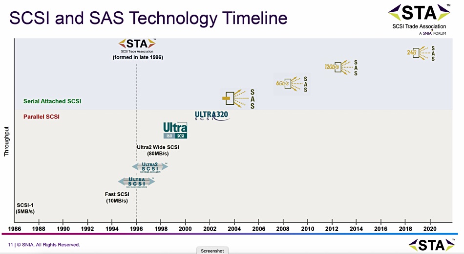
Prepare for nested acronym deconstruction: SAS (Serial Attached SCSI, or Small Computer Systems Interface) is an interconnect used by disk drives and SSDs. It is used along with SATA (Serial Advanced Technology Attachment) and both have replaced PATA (Parallel Advanced Technology Attachment). PATA, by today’s standards is slow, transferring data at up to 133 MBPs and supporting 80GB capacity drives. SATA is faster, transferring data at up to 300 MBps.
The current SATA standard, revision 3, defines a 6 Gbps bandwidth.
SCSI represents an upgrade to PATA and SATA as it is used for additional peripheral devices such as printers and scanners.
The SAS revision 3 or SAS-3 standard defines a 12 Gbps interface bandwidth, which matched the PCIe 3 interconnect to which SAS drives ultimately connected. SAS-4 or 24G SAS, the current standard, moves this up to 24 Gbps, and was defined by the STA in 2019/2020. It was prompted in part by the then coming PCIe 4 interface with its doubled speed over PCIe 3.
Brett said of SAS-3: “SAS/SCSI was optimized for HDDs at the time, since SSDs were not around yet. Steps have been taken over time to accommodate SSDs and take better advantage of their performance. NVMe was created from the ground up for flash-based storage, so it is better optimized for SSDs.”
SAS-3 can run over a longer cable, 12m, than SATA’s 1m length. SAS connectors support SATA connectivity but the reverse is not true.
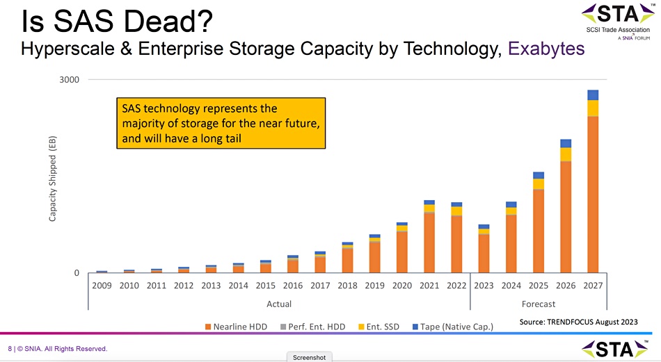
An STA/TrendFocus chart shows that the bulk of enterprise storage capacity is represented by nearline drives and the bulk of these use the 12 Gbps SAS interface:
There are no 24G SAS disk drives and only a few 24G SAS SSD products made by enterprise storage suppliers, as the NVMe (Non-Volatile Memory Express) interconnect has taken over the SSD interface area, and high-speed disk drives, operating at the 10,000rpm level are being replaced by SSDs. That leaves the bulk of the enterprise and PC disk drive products spinning at 7,200rpm and quite happily connecting at the 12gig SAS level.
A few 24G SAS SSD products are appearing on the market – for example, Kioxia PM6 and PM7, and Samsung’s PM1653. There are various 24G SAS interconnect products, such as Broadcom’s 9600 series interfaces, plus cables, connectors, analyzers and extenders. But, by and large, 24G SAS adoption by storage drive manufacturers has been slow.
Brett however, characterized SAS as immortal, because it has such an entrenched hold in the disk drive interconnect area. He thinks SAS will be the majority HDD interface through to 2027. NVMe, which, with the NVMe v2.0 spec, has developing a disk drive extension, may eat into SAS’s disk drive hegemony over time. But the massive SAS HDD base will provide a replenishment and upgrade market that will endure for many years.
He pointed out that NVMe is optimized for flash whereas SAS is optimized for disk. With NVMe you can have four PCIe lanes on an SSD compared to single or dual SAS lanes, making the NVMe interface much faster.
The next SAS standard, which is being worked on now, will be 24G+, with a 2025/2026 definition data. Brett did say that there is no doubling of 24G speed, to 48 Gbps, being envisaged, and no 4-port SAS interface being developed. Our understanding is that 24G+ will continue to use the SAS-4 physical layer spec, and this implies no increase in speed beyond 24 Gbps. We have asked Brett to confirm this, and he said: “Yes. 24G+ will have the same physical interface speed as 24G (SAS-4) @ 22.5Gbps.”
The STA has defined 24G+ command duration limits, format wish presets and logical depopulation. It is considering attenuation, key per IO, growing the protection information field and making fairness enhancements with the 24G+ standard.
Although the STA is ceding the high-speed drive interface area to NVMe it sees a continuing role for SAS in hyperscale storage environments. Brett cited the Open Compute Project’s drive chassis standards as evidence; Knox (6Gbps SAS) in 2013, Honey Badger (12 Gbps SAS) in 2015, Bryce Canyon (12 Gbps SAS) in 2017, and Grand Canyon (14 Gbps SAS) in 2022. He thinks there will be follow ons for at least two generations, and they may well use 24G+ SAS.
Brett reckons SAS has been the dominant storage interface for nearly two decades and will be so for years to come. The STA is, he said, ensuring that SAS will continue to innovate to meet evolving datacenter needs.
Bootnote
Although 24G SAS is nominally a 24 Gbps standard each lane in a 24G SAS interconnect actually operate at 22.5 Gbps
Project Silica, a Microsoft plan to store multiple layers of archival data inside slabs of quartz glass, is getting closer to becoming a product, as a 16-page document explains.
Microsoft’s update of its glass archival storage project is an academic paper submitted to the 29th ACM Symposium on Operating System Principles (SOSP 2023).
The aim is to develop a cloud-scale archive media system for reading and writing data. The encoding technology is the production of areas with polarization-based patterns at points within a square glass slab, defined by 3D coordinates, and there can be hundreds of layers.
These polarization pattern points are called voxels, which are produced using femtosecond laser pulses. Each voxel encodes 3 to 4 bits of data. Voxels are written side by side in 2D layers across the platter’s XY plane. They are organized into rectangular sectors, a 2D group of 100,000+ voxels in an XY plane, about 100 KB of data. A 3D set of sectors is called a track and there can be multiple TB of data per platter.
This is somewhat similar to Cerabyte’s technology, which also uses femtosecond laser pulses to create physical changes in a ceramic coating on square glass slabs. The changes are nano-scale holes, like a high-technology punch card. But Cerabyte’s holes are generated as part of QR codes whereas Project Silica’s voxels are laid down in tracks. Its slabs are placed on a platform that moves from left to right and forward-backward underneath read and write head devices (lasers and polarization microscopes). Cerabyte’s glass carrier only moves forward and backward, and is a single layer medium. Therefore, Project Silica glass is a random-access medium.
Both Cerabyte and Microsoft envisage library racks to hold the data storage medium – in cartridges holding square glass data carriers in Cerabyte’s design, but as raw quartz glass slabs in Microsoft’s library. This library has a robotic transfer system composed of several independent and battery-powered robot pickers (shuttles), a small swarm as it were, with the ability to flip up and down vertically between multiple horizontal rails running through the library racks to the read and write racks. A video demonstrates this. Microsoft likens it to “a set of free roaming shuttles inspired by state-of-the-art warehouse robotic systems.”
Two independent robot pickers in Microsoft’s Project Silica library
Microsoft says: “The read drive scans sectors in a single swift Z-pattern, and the resulting images are processed for decoding. Different read drive options offer varying throughput, balancing cost and performance.”
There are physically different read and write drives in the Project Silica system.
There is a one-way system between the write racks and the library racks to prevent a platter being overwritten. Like Cerabyte, the Project Silica technology is inherently write-once only. It’s a physical WORM system. Microsoft says: “The robotics are unable to insert a glass platter into a write device once the glass media has been written.” That means there is a physical air gap at library system level, and also that glass platters are written to full capacity in one operation, from the deepest to the top layer.
The write drive is full rack-sized and writes multiple platters concurrently; ditto the read drive rack which contains multiple drives. Both read and write drive racks require cooling, power, and network connectivity.
Written platters are read (verified) before being stored in the library. That means a freshly written drive is transferred by shuttle to a read drive. The Microsoft paper states: “To enable high drive efficiency, two platters can be mounted simultaneously in a read drive; one undergoing verification, and one servicing a customer read. Customer traffic is prioritized over verification.”
Read (scanned) Project Silica voxel images are passed through a machine learning algorithm to turn them into binary data. The read drive seeks on the XY plane to locate a desired track then reads an entire track’s sectors in a single scan in the Z (depth) direction. The read drive throughput scales in multiples of 30 MBps.
Microsoft’s researchers analyzed Azure archive IO patterns and found that small file IOs dominated (256 MiB to 256 GiB) along with significant differences at a datacenter level. This means that “minimizing the latency of mechanical movement in the library is crucial for optimal performance,” and also that a Silica library should be customizable for different workload patterns.
The Project Silica library system uses two error coding techniques – LDPC (Low Density Parity Check) inter-sector error coding and NC (Network Erasure Coding), with within-track, large group (multi-track), and cross-platter NC variants employed.
The Silica library’s read performance, the delay between the reception of a read request, and the last byte read and sent from the library is defined by the 99.9th percentile; the tail completion time. Microsoft assumes “an SLO of 15 hours to the last byte, which is in line with current archival services.”
This completion time does not include the disaggregated decode by the machine learning algorithms, however.
Microsoft’s paper concludes: “The unique properties of the glass media and the clean slate, cloud-first co-design of the hardware and software allow Silica to be fundamentally more sustainable and achieve significantly lower costs for archival data than magnetic tape.”
Comment
This glass-based archive represents the first credible tape archive replacement technology we have seen, being far more realistic than DNA storage. Microsoft and Cerabyte are working on tape archive replacement technologies that could result in a deliverable product within five years. Tape companies should be looking at this technology to see how they might incorporate it in their product planning roadmaps.
Nebulon has developed a Data Processing Unit (DPU) specifically for edge servers, enabling their CPUs to fully focus on running applications.
A couple of weeks after launching its Medusa2 DPU for datacenter servers, Nebulon unveiled a prototype of the physically smaller Medusa2i card at a TechLive event in London. DPUs take care of storage, network, security, and management functions for host x86 servers, releasing CPU cycles for app processing. Nebulon developed its Medusa2 DPU from an earlier SPU (Services Processing Unit) focused on server management and security.
Interestingly, Nebulon positions its Medusa2 card as a way of having servers that compete with hyperconverged infrastructure (HCI) systems running vSphere/vSAN or KVM. In Nebulon COO and co-founder Craig Nunes’ view, “3-tier enterprise customers are adopting servers plus DPUs, basically skipping over HCI.”
We asked if DPUs could be used to build a more efficient HCI system and Nunes agreed. “One hundred percent,” he said, noting that “a software stack would be needed.”
Technical director Phil Hooker said: “The DPU is connected to storage drives in server (like SPU cards). There’s no RAID card – we replace it. Ninety percent of customers use us as a boot device.”
Prototype Medusa2i card
He said the Medusa2i card was, like Medusa2, based on Nvidia’s BlueField3 technology, but has half the CPU cores (8 instead of 16) and half the memory of Medusa2 (24 instead of 48GB), and is physically smaller. It can carry 4 x M.2 SSDs with 2-32 TB capacity.
The interest in developing it was sparked by Nebulon’s four server OEMs – Dell, HPE, Lenovo, and Supermicro. They envisaged non-rackmount server use cases enabling edge and remote sites to get the same storage, networking, and CPU offload benefits as well as remote fleet management. Nebulon started developing Medusa2i about a quarter after Medusa2 development began.
Nunes pointed out that an edge server so equipped could have no local storage apart from what’s on the Medusa2i card, and that makes it effectively a hyperconverged system.
Nebulon has a 4-port Medusa2 card coming, doubling bandwidth to 400 Gbps from an initial 2-port x 200Gbps. Nunes added that applications or other software could run on the Medusa2’s Arm cores.
He reckons interest in Medusa2 “is off the chart.” The card is currently assembled in the US, but if volumes surpass the 10,000 units level off-shore manufacturing could become a possibility.
Comment
Nebulon is at a crossing-the-chasm moment. If its OEMs start selling large numbers of Nebulon DPU-equipped servers because their enterprise customers see the benefits of more application code cycles, lower licensing costs, enhanced security, and better server management, the company could face a step change in its fortunes.
Startup Cerabyte, which specializes in ceramic-coated glass storage, has built a demo workflow system and is looking for funding and partners to take the concept further.
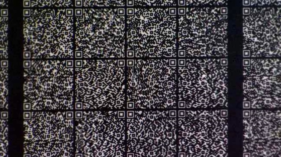
The German company has technology to create microscopic holes in a layer of a ceramic substance coating a square glass carrier. Holes are created with femtosecond laser pulses and laid down in a format similar to quick response (QR) codes with sequences of holes and no-holes representing binary zeroes and ones.
QR pattern data blocks written in ceramic layer on Cerabyte’s glass carrier
The glass carrier can be coated on both sides to increase data capacity, and several can be stacked inside a data cartridge. Cerabyte envisages a storage system composed of library racks and a write-read rack, with robotics used to transport the cartridges from the library racks to the write-read rack.
It could be likened to a tape library with the tape drives replaced by glass cartridge writer/reader devices, or an optical storage jukebox.
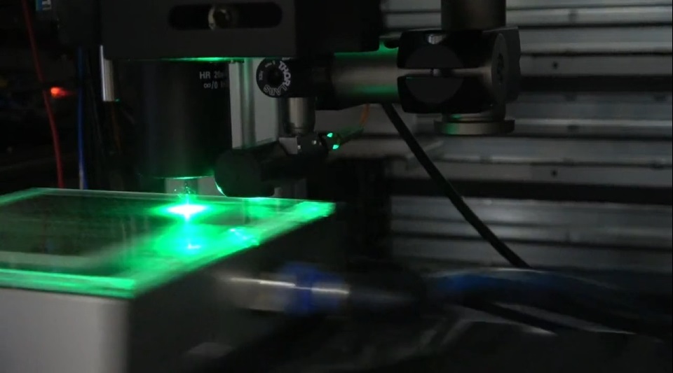
The demo Cerabyte system uses a datacenter rack form factor, and is shown in a video. The commentary explains that once a cartridge is brought to the write-read device, a carrier is extracted and placed on a platform or stage. This can move forward or backward underneath laser and reading camera components. These are focused on the glass carrier using mirrors and lenses.
The video commentary explains: “During the forward movement of the stage, a line of QR patterns is written, which are read back and verified during the backwards movement by a microscope camera. When a data carrier is fully written, it is returned into the cartridge which is then moved back to library.”
“The read workflow is similar whereby only the microscope camera is engaged and data is read in both directions of the stage movement. Error Correction and file allocation will work similar to other mainstream data storage technologies.”
We can readily understand that the write speed is based on two stage movements, forward for writing and backward for reading. Reading is based on both forward and backward movements.
The TBps write and read speeds will depend upon the QR code density. Cerabyte has mentioned 1 PB cartridges as a potential initial capacity with development through 10PB and out to 100 PB by using smaller bit sizes (holes) in the ceramic recording medium. It has discussed a progression from 100 nm to 3 nm bit sizes.
This ceramic medium has an initial thickness of 50 to 100 atoms and is said to be resistant to fire, cold, water, radiation, electricity, and other effects that can destroy data on tapes, disk drives, and SSDs. The glass carriers effectively last forever – we’re told – and, once in their cartridges, need no electrical energy for cooling or data maintenance. Moreover, unlike archival tape cartridges that require re-silvering, these carriers do not need any form of refreshing.
Cerabyte says its demo system was manufactured using commercial off-the-shelf components. Interested potential manufacturing partners, enterprises, research institutions, and institutional investors should contact Cerabyte by email at office@cerabyte.com.
Comment
The obvious comparisons we make with Cerabyte’s technology are Blu-ray optical disks and holographic storage technologies. Blu-ray writing creates pits in a recording medium which can be multi-layered. The spot size for the blue laser used is 580 nm with a 150 nm pit size. The pits are laid down in circular tracks on disks, whereas Cerabyte uses QR blocks on square glass carriers and has a smaller pit (hole) size of 100 nm. Holographic storage technology has never resulted in a commercial product due to manufacturing difficulties around the highly precise mirrors and lenses required.
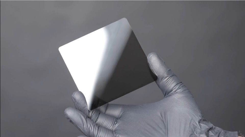
The data capacity of Cerabyte’s demonstration square glass carriers or physical size is not known. The video suggests they are about 2-3 inches squared:
Microsoft has a Project Silica research effort looking at a glass-based archival storage medium and system for its Azure public cloud.
Remote large file collaboration startup LucidLink has raised $75 million to engineer software for distributed creative professionals to work faster together.
Update. CTERA CTO comments added; 27 November 2023.
LucidLink’s FileSpaces product has file sections streamed directly from a central cloud repository rather than being synchronized and shared between remote worker locations. This sync ‘n’ share approach is how it characterizes the services offered by CTERA, Egnyte, Nasuni, and Panzura. LucidLink says its software provides fast access to large files used by customers such as Adobe, A&E Networks, Whirlpool, Shopify, Buzzfeed, Spotify, various Hollywood studios, major broadcasters, digital ad agencies, architectural firms, and gaming companies.
Peter Thompson
Peter Thompson, LucidLink co-founder and CEO, said: “Legacy collaboration and storage solutions are not designed for this new hybrid workplace reality, and LucidLink is becoming the go-to solution for companies looking to future-proof their businesses. Our customers are reaching 5x in productivity gains on previously impossible workflows, and we are excited to see how they continue to unlock new possibilities as we help to accelerate the future of collaborative work.”
LucidLink was founded in 2016 and the latest C-round funding follows a $20 million B-round last year, taking the total raised to about $115 million. The round was led by growth stage investor Brighton Park Capital. Several existing investors – including Headline, Baseline Ventures, and Adobe Ventures – also participated. The new capital will be put into product and engineering development, customer acquisition efforts, and expansion into new verticals and geographies.
Co-founder and CTO George Dochev said: “With this Series C investment, LucidLink will accelerate its most ambitious product updates in the Company’s history to expand our technology leadership position, open up new customer use cases, and create more personalized product experiences that enable creative professionals to work more efficiently and effectively.”
The startup has grown its annual recurring revenue (ARR) by nearly 5x and the number of users on its platform by more than 4x in the past two years. LucidLink says that, for creative industries that work with complex files and applications, real-time collaboration across a hybrid and remote employee base has become a major concern. It cites as an example that three-quarters of creative collaboration now happens remotely, with the average creative review process taking eight days and more than three versions to receive sign-off, according to a Filestage report.
LucidLink says that IDC predicts that investment in cloud infrastructure and services will grow to $1.2 trillion by 2027 as the need for businesses to prepare for a hybrid workforce grows more urgent.
It is uncertain at what point file collaboration services like CTERA, Egnyte, Nasuni, and Panzura no longer meet customer needs and where LucidLink’s technology becomes the more suitable option. All LucidLink says is that its creative professional customers get faster access to large files, but what does “faster” and “large” mean?
GigaOm analysts said in September 2021: “LucidLink focuses on globally, instantly accessible data with one particularity – data is streamed as it is read. Streaming makes the solution especially well suited for industries and use cases that rely on remote access to massive, multi-terabyte files, such as the media and entertainment industry. LucidLink’s capabilities in this area are unmatched.”
A blogpost by Thompson and Dochev discusses the new funding and what it means.
Update
CTERA CTO Aron Brand suggests LucidLink is incorrect in its claim to be the only player in the market to have this streaming support technology. “CTERA’s streaming technology, especially the dedicated integrations with the Adobe suite including CTERA for Adobe Premiere, Illustrator, Photoshop, and InDesign,” he says, “has been a game-changer for its clients.” There are video demonstrations here.
Brand tells us some of CTERA’s largest clients, such as WPP and Publicis, benefit from CTERA’s offerings. Its edge filers, providing more than just an agent-based solution (which is what CTERA believes LucidLink offers), offer features such as up to 256TB of fast local cache, useful for 8K video production, and “enabling professional level of operation that is simply impossible with agent-based solutions.” For WPP, CTERA Edge Filers enabled it to achieve gains in productivity, collaboration, and cost savings.
Additionally, the CTERA Mac Assist enhances the user experience of Mac designers interacting with the global filesystem.
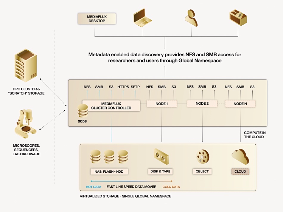
Arcitecta has upgraded its Mediaflux software to become a Universal Data System orchestrating, managing, and storing geo-distributed unstructured data across its entire lifecycle.
Mediaflux is an unstructured data silo-aggregating software abstraction layer with a single namespace that can store files and objects in on-premises SSDs, disk or tape, or the public cloud, with a database holding compressed metadata. There is a fast Mediaflux data mover to put files in the appropriate storage tier.
Mark Nossokoff, Cloud & Storage lead analyst at Hyperion Research, said in a statement: “By working to converge data management, orchestration, and storage onto a single unified platform, Arcitecta is aiming to boost users’ data accessibility, manageability, and scalability. And with pricing based on concurrent users rather than on capacity-based data volumes being managed, and eliminating the need for third-party software and file systems, Arcitecta is also seeking to significantly lower their customers’ costs.”
Up until now enterprise and most organizational files have been stored in clustered systems using dual controller nodes, with objects stored in scale-out systems. High-performance computing (HPC) systems have used parallel file systems such as Lustre and Storage Scale (GPFS). As file and object storage capacity needs have increased from terabytes to petabytes and on to exabytes, a need rose for lifecycle management software to analyze an organization’s unstructured data estate and move less-accessed data from fast and expensive storage to less expensive but slower tiers, such as from SSD to disk, and then on to tape or to object storage, on-premises or in the public clouds. Komprise is an active supplier in this area.
Public cloud object stores have been used as a basis on which to provide file collaboration between remote users. Suppliers such as CTERA, Egnyte, Nasuni and Panzura are specialists in this sphere.
Another need is now growing, and that is a requirement to be able to navigate an unstructured data estate composed of billions of files and objects that can be global in scope and used by distributed and remote offices. This has given rise to data orchestrators, predominantly Hammerspace, which manages sophisticated metadata repositories and enable access to globally distributed files as if they are local.
Now along comes Arcitecta saying you don’t need these extra software layers. Its Mediaflux metadata-driven software can do it all.
Arcitecta graphic modified for readability
It claims its Mediaflux Universal Data System can provide:
Converging data management, orchestration and storage within a single platform to allow customers to access, manage, and utilize data assets more effectively.
Manage every aspect of the data lifecycle, both on-premises and in the public cloud, with globally distributed access, providing cataloging, transformation, dissemination, preservation, and eventual storage. This streamlines the processes as data moves through its lifecycle.
Multi-protocol access and support with NFS, SMB, S3, SFTP and DICOM, providing flexible access and interoperability. Its global distributed access ensures data can be retrieved from any location, facilitating international collaboration among data-intensive organizations such as research facilities, universities, entertainment studios, and government institutions.
Scalability as Mediaflux licensing, based on the number of concurrent users, is decoupled from the volume of data stored so organizations can affordably scale storage needs to hundreds of petabytes, accommodating hundreds of billions of files without the financial strain typically associated with such vast capacities.
Clustered storage capabilities without the need for third-party software, whether a business is using block storage from one vendor or multiple vendors, and Mediaflux can integrate and manage all the data and storage within the environment.
Cost savings by eliminating the need for third-party software, storage fabrics and volume-based pricing. Mediaflux’s intelligent data placement feature optimizes storage efficiency by automatically tiering data based on usage and access patterns.
Supports multi-vendor storage environments, allowing customers to choose best-of-breed hardware. The storage underlying the Mediaflux Universal Data System can be from any vendor or multiple vendors.
Fast file transfer with integrated high-speed WAN file transfer features, with throughput of up to 95 percent of the available bandwidth on networks of 100 GbitE or more. Metadata and adaptive compression capabilities increase speed by eliminating redundant file and data transfers for optimized data movement.
Arcitecta also claims that, despite having fast file transfer, Mediaflux can take compute operations directly to the data without moving the data over a network. With a direct path approach, users can collaborate more effectively with a system that distributes compute algorithms to where the data resides. This approach is important since transmitting data over large distances is expensive and inefficient.
Hammerspace also recognizes that transmitting data over large distances is expensive and time-consuming and has a partnership with Vcinity to deal with the problem.
Jason Lohrey
The Mediaflux Universal Data System is available immediately. There is a Solution Brief here and some webpages on the Mediaflux Universal Data System here if you would like to find more.
Jason Lohrey, CEO and Arcitecta founder, commented: “Mediaflux Universal Data System is the culmination of Arcitecta’s vision for the future of data management. By merging world-class data management, orchestration, multi-protocol access, and storage into one cohesive platform, we aim to set a new industry standard that moves beyond data storage and makes data more accessible, manageable and valuable than ever before.”
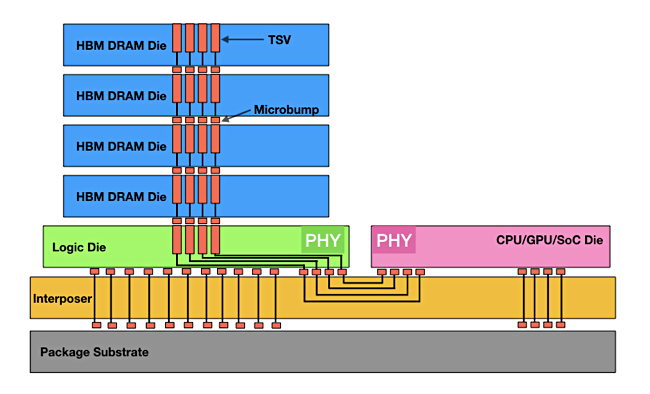
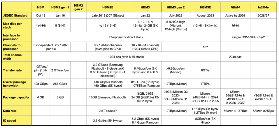
Accelerated processors like GPUs could get faster memory access by using light-based data transfer and by directly mounting High Bandwidth Memory (HBM) on a processor die.
HBM came into being to provide more memory to GPUs and other processors than the standard x86 sockets interface could support. But GPUs are getting more powerful and need data accessed from memory even faster in order to shorten application processing times – Large Language Models (LLMs) for example, can involve repeated access to billions if not trillions of parameters in machine learning training runs that can take hours or days to complete.
Current HBM follows a fairly standard design: a stack of HBM memory is connected to an interposer, placed on a base package layer, via microbumps which link to Through Silicon Vias (TSVs or connecting holes) in the HBM stack. The interposer also has a processor mounted on it and provides the HBM-to-processor connectivity
HBM suppliers and the HBM standards body are looking at ways to speed HBM-to-processor access speeds by using technologies such as photonics or directly mounting the HBM on the processor die. The suppliers are setting the HBM bandwidth and capacity pace – seemingly faster than the JEDEC standards body can keep up.
The current standard is called HBM3e, and there are mooted HBM4 and HBM4e follow-on standards.
Samsung
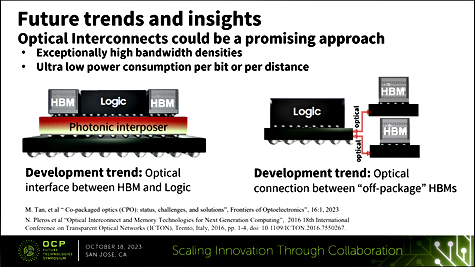
Samsung is investigating the use of photonics in the interposer, with photons flowing across the links faster than bits encoded as electrons, and using less power. The photonic link could operate at femtosecond speeds. That means a 10⁻¹⁵ unit of time – one quadrillionth (one millionth of one billionth) of a second. The Korean behemoth’s Advanced Packaging Team, featuring principal engineer Yan Li, presented on this topic at the recent Open Compute Project (OCP) summit event.
Samsung presentation at OCP Global Summit 2023. See the slide deck here.
An alternative to using a Photonics Interposer is to link the HBM stacks more directly to the processor (logic in Samsung diagram above). This is going to involve careful thermal management to prevent over-heating. This could mean that the HBM stacks could be upgraded over time to provide more capacity, but there would need to be an industry standard covering that area for it to be possible.
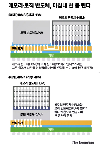
SK hynix
SK hynix is also working on a direct HBM-logic connection concept, according to a report in the Korean JoonAng media outlet. This notion has the GPU die or chip manufactured with the HBM chip in a mixed-use semiconductor. The chip shop views this as an HBM4 technology and is talking with Nvidia and other logic semiconductor suppliers. The idea involves the memory and the logic manufacturers co-designing the chip, which is then built by a fab operator such as TSMC.
This is somewhat similar to the Processing-in-Memory (PIM) idea and, unless safeguarded by industry standrards, will be proprietary with supplier lock-in prospects.
Together Samsung and SK account for more than 90 percent of the global HBM market.
Micron
Tom’s Hardware reports that Micron – the rest of the market – has HBM4 and HBM4e activities. It is currently making HBM3e gen-2 memory with 24GB chips using an 8-high stack. Micron’s 12-high stack with 36GB capacity will begin sampling in the first quarter of 2024. It is working with semiconductor foundry operator TSMC to get its gen-2 HBM3e used in AI and HPC design applications.
Micron says its current product is power-efficient and, for an installation of ten million GPUs, every five watts of power savings per HBM cube (stack) is estimated to save operational expenses of up to $550 million over five years over alternative HBM products. These strike us as somewhat fanciful numbers.
The HBM4 standard should arrive by 2026 and have a double-width interface of 2,048 bits compared to HBM3e’s 1,024 bits, with a per-stack bandwidth of more than 1.5TB/sec. HBM3e products operate in the 1.15 and 1.2 TB/sec area. Micron thinks there will be 36GB 12-high stack HBM4 capacity as well as 48GB 16-high stacks.
The table below adds Micron’s HBM4 and follow-on HBM4e (extended) numbers to the existing HBM – HBM3e numbers that we have.
B&F Table. HBM4 and HBM4e entroes are in italics because they are not official JEDEC standards.
Comment
Micron is not talking about combining HBM and logic in a single die, unlike Samsung and SK hynix. It will be telling the GPU suppliers – AMD, Intel and Nvidia – that they can get faster memory access with a combined HBM-GPU chip, while the GPU suppliers will be well ware if the proprietary lock-in and single source dangers.
As ML training models get larger and training times lengthen, the pressure to cut run times by speeding memory access and increase per-GPU memory capacity will increase in lockstep. Throwing out the competitive supply advantages that exist with standardized DRAM to get locked-in HBM-GPU combined chip designs – albeit with better speed and capacity – may not be the right way to move forward.