


Accelerated processors like GPUs could get faster memory access by using light-based data transfer and by directly mounting High Bandwidth Memory (HBM) on a processor die.
HBM came into being to provide more memory to GPUs and other processors than the standard x86 sockets interface could support. But GPUs are getting more powerful and need data accessed from memory even faster in order to shorten application processing times – Large Language Models (LLMs) for example, can involve repeated access to billions if not trillions of parameters in machine learning training runs that can take hours or days to complete.
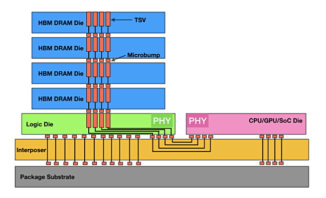
Current HBM follows a fairly standard design: a stack of HBM memory is connected to an interposer, placed on a base package layer, via microbumps which link to Through Silicon Vias (TSVs or connecting holes) in the HBM stack. The interposer also has a processor mounted on it and provides the HBM-to-processor connectivity
HBM suppliers and the HBM standards body are looking at ways to speed HBM-to-processor access speeds by using technologies such as photonics or directly mounting the HBM on the processor die. The suppliers are setting the HBM bandwidth and capacity pace – seemingly faster than the JEDEC standards body can keep up.
The current standard is called HBM3e, and there are mooted HBM4 and HBM4e follow-on standards.
Samsung
Samsung is investigating the use of photonics in the interposer, with photons flowing across the links faster than bits encoded as electrons, and using less power. The photonic link could operate at femtosecond speeds. That means a 10⁻¹⁵ unit of time – one quadrillionth (one millionth of one billionth) of a second. The Korean behemoth’s Advanced Packaging Team, featuring principal engineer Yan Li, presented on this topic at the recent Open Compute Project (OCP) summit event.

An alternative to using a Photonics Interposer is to link the HBM stacks more directly to the processor (logic in Samsung diagram above). This is going to involve careful thermal management to prevent over-heating. This could mean that the HBM stacks could be upgraded over time to provide more capacity, but there would need to be an industry standard covering that area for it to be possible.
SK hynix
SK hynix is also working on a direct HBM-logic connection concept, according to a report in the Korean JoonAng media outlet. This notion has the GPU die or chip manufactured with the HBM chip in a mixed-use semiconductor. The chip shop views this as an HBM4 technology and is talking with Nvidia and other logic semiconductor suppliers. The idea involves the memory and the logic manufacturers co-designing the chip, which is then built by a fab operator such as TSMC.
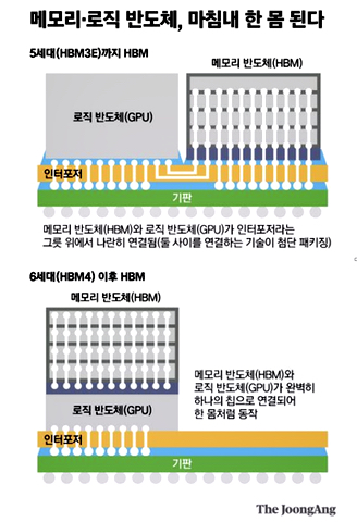
This is somewhat similar to the Processing-in-Memory (PIM) idea and, unless safeguarded by industry standrards, will be proprietary with supplier lock-in prospects.
Together Samsung and SK account for more than 90 percent of the global HBM market.
Micron
Tom’s Hardware reports that Micron – the rest of the market – has HBM4 and HBM4e activities. It is currently making HBM3e gen-2 memory with 24GB chips using an 8-high stack. Micron’s 12-high stack with 36GB capacity will begin sampling in the first quarter of 2024. It is working with semiconductor foundry operator TSMC to get its gen-2 HBM3e used in AI and HPC design applications.
Micron says its current product is power-efficient and, for an installation of ten million GPUs, every five watts of power savings per HBM cube (stack) is estimated to save operational expenses of up to $550 million over five years over alternative HBM products. These strike us as somewhat fanciful numbers.
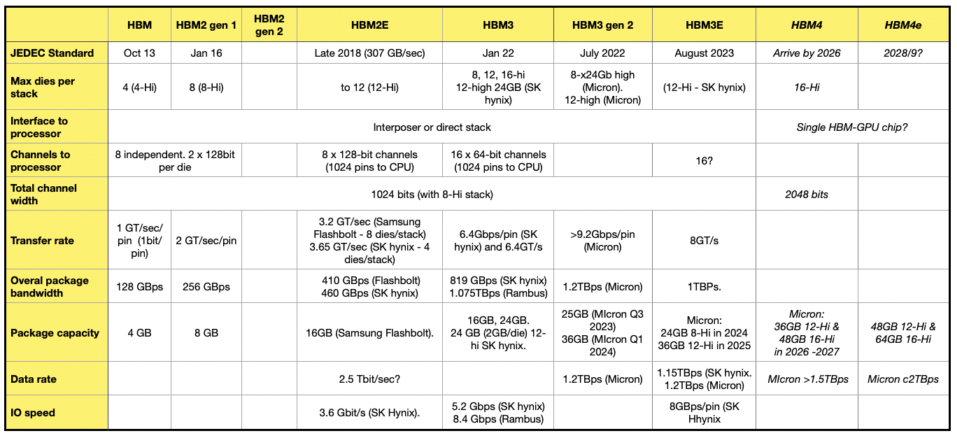
The HBM4 standard should arrive by 2026 and have a double-width interface of 2,048 bits compared to HBM3e’s 1,024 bits, with a per-stack bandwidth of more than 1.5TB/sec. HBM3e products operate in the 1.15 and 1.2 TB/sec area. Micron thinks there will be 36GB 12-high stack HBM4 capacity as well as 48GB 16-high stacks.
The table below adds Micron’s HBM4 and follow-on HBM4e (extended) numbers to the existing HBM – HBM3e numbers that we have.
Comment
Micron is not talking about combining HBM and logic in a single die, unlike Samsung and SK hynix. It will be telling the GPU suppliers – AMD, Intel and Nvidia – that they can get faster memory access with a combined HBM-GPU chip, while the GPU suppliers will be well ware if the proprietary lock-in and single source dangers.
As ML training models get larger and training times lengthen, the pressure to cut run times by speeding memory access and increase per-GPU memory capacity will increase in lockstep. Throwing out the competitive supply advantages that exist with standardized DRAM to get locked-in HBM-GPU combined chip designs – albeit with better speed and capacity – may not be the right way to move forward.


