Home Blog Page 181

VergeIO adds GPUs to virtual datacenter systems

Verge.io, the revitalized and renamed Yottabyte, has added GPU virtualization to its virtual datacenter software take on HCI and composable systems.

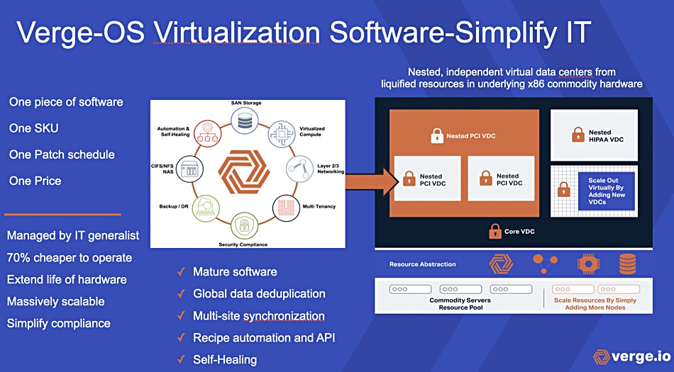
HCI (hyperconverged infrastructure) builds an IT datacenter from standard server-storage-networking boxes with storage pooled across them like a virtual SAN. Verge.io software does the same but then subdivides the pooled compute-storage-networking resource, the abstracted datacenter, into virtual datacenters (VDCs). These can be used by customers of its MSP clients. Such MSPs can create VDCs from a master VDC and nest them so that their customers experience a dedicated datacenter from what is actually a shared MSP VDC resource.

Verge.io CEO Yan Ness said: “Our users are increasingly needing GPU performance, from scientific research to machine learning, so vGPU and GPU Passthrough are simple ways to share and pool GPU resources as they do with the rest of their processing capabilities.”

Verge.io slide

The company’s software allows users and applications with access to a virtual datacenter to share the computing resources of a single GPU-equipped server. Users and/or administrators can create a virtual machine with pass-through access to that GPU and its resources. 

Alternatively, Verge.io can manage the virtualization of the GPU and serve up virtual GPUs (vGPUs) to virtual datacenters, manageable on the same platform as all other VDC shared resources.

Verge.io slide

Servers in a VDC run the Verge-OS and it encapsulates a datacenter. The storage drive copy of this can be snapshotted then replicated to other servers, with global deduplication reducing data amounts. Verge-OS instances are patched in a single operation, making them simpler to maintain than some HCI software products.

Darren Pulsipher, Intel’s chief solution architect of public sector, commented: “The market is looking for simplicity, and Verge-OS is like an ‘Easy Button’ for creating a virtual cloud that is so much faster and easier to set up than a private cloud. With Verge-OS, my customers can migrate and manage their datacenters anywhere and upgrade their hardware with zero downtime.”

Customers need to obtain an Nvidia license for running the GPU hardware as part of Verge.io’s system.

Verge.io and composable systems

By carving up its overall VDC resource into sub-VDCs, Verge.io is effectively composing datacenters. Ness says that composable server systems software, such as that from Liqid, is aimed at preventing servers having stranded component resources, such as compute or flash storage, and maximizing its use by making it shareable. The focus of such composed systems is an application.

The focus of Verge.io’s “composed” VDCs is an MSP customer or end user who needs to run a set of applications, not one. A VDC could be set up for a single application, such as VDI, but is more commonly set up to run several. The focus is on datacenter administration simplicity and effectiveness, not resource stranding.

Comment

Yottabyte ran into problems, described here. By the end of 2018 it had been rebranded as Verge.io. Then new investors came on board, including Ness, who came out of retirement. They saw great potential in the business’s software but thought it needed redirecting to new markets, meaning MSPs, universities, and enterprises in that order. A key attribute of the software is its simplicity of management and use. They pruned the business setup, bought a new and reduced but more focused sales organisation on board, and set out on a new course.

Verge,io slide

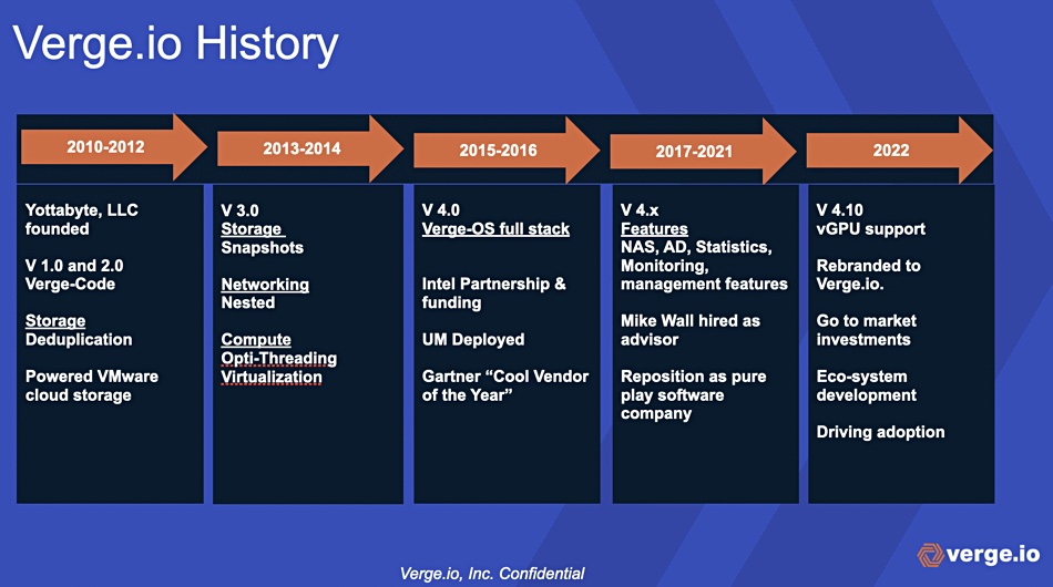
It currently has around 15 employees. There used to be 50. Ness said: “We tore it down to only what we need.” It has some 45 customers. Verge.io is now, Ness says, a startup with a mature product. This small company is set on punching well above its weight.

Cloudian balances object storage access loads

Cloudian bezel
Cloudian bezel

Object storage supplier Cloudian has launched a load-balancing product called HyperBalance.

Update; Cloudian HW/SW to SW-only OEM Loadbalancer.org deal change date added. 19 Aug 2022.

Cloudian’s HyperStore is scale-out object storage software that runs on x86 servers, inside virtual machines, in container environments, on the public cloud and in Cloudian’s own 1000, 1600 and 4200 appliances with 100TB to 1PB+ capacities. Load balancing improves responsiveness and increases the availability of applications by distributing network or application traffic across a cluster of servers. It also facilitates the storage of data in multiple locations for zero downtime in case one location fails and a switchover is needed.

Cloudian says that, in its shared-nothing architecture, any storage node can respond to any incoming request, providing a parallel processing capability that allows performance to grow as new nodes are added. But individual nodes can get overwhelmed and become a bottleneck. HyperBalance helps avoid this and achieve maximum performance by evenly distributing workload across all nodes, thereby eliminating bottlenecks.

It establishes a clean separation between the HyperStore object storage domain and the accessing networking infrastructure. The HyperStore distributed system gets a single IP address and is accessed and used as a private storage cloud.

Cloudian Loadbalancer appliance
Loadbalancer appliance

Cloudian’s HyperBalance appliance is based on Loadbalancer.org’s enterprise product line and operates at layer 7 in the OSI stack. Loadbalancer.org has Enterprise 1G, 10G, 25G, 40G, 50G and 100G appliances with the number representing the level of Ethernet connectivity. The Enterprise 40G appliance has an eight-core XEON CPU and provides 48Gb/sec throughput and 19,584 SSL TPS.

Loadbalancer works with a number of object storage vendors, including Hitachi Vantara and MinIO. Cloudian said told us: “Although Loadbalancer has six appliances, we’re only OEM’ing their software
(no hardware) and offering our own 50GbitE and 100GbitE appliances as well as a 10GbitE software VM version.” This is a change from the University of Leicester situation where actual Loadbalancer.org hardware was used. A Cloudian spokesperson said: “The change to OEM’ing only their software became effective as of this Tuesday when we made our announcement.”

HyperBalance provides high availability and is a scale-out technology. It can handle up to handle 3.3GB of storage per second with no impact on performance. The University of Leicester in the UK is a customer, and has two HyperBalance appliances [Enterprise 40G products] installed as a high-availability pair across two datacenters. Starting with 12 HPE Apollo servers, they now balance traffic across 15 Apollos and handle an average of 120TB  per week.

The two HyperBalance boxes are configured as a secure gateway to interconnect the Cloudian HyperStore network to external services on the university’s public network.

Support for the University of Leicester is provided by Loadbalancer.org. Check out a downloadable Loadbalancer.org white paper here.

Talking about an AI revolution? Don’t forget the storage

Sponsored GPUs have revolutionized AI and HPC over the last decade. But they didn’t do this on their own.

The AI and HPC boom could not have happened without massive amounts of data, requiring corresponding leaps in file system and storage technology.

So, what is the state of the art today? What effect will the hybrid cloud era have? And where do new technologies like DPUs and NVM Express over Fabric fit in?

You can get on top of all these questions in this Open Storage Summit Session, Feeding the Data-Hungry GPU Beast, on September 1, 10am PT / 1pm ET / 6pm BST.

The Register’s Tim Prickett Morgan will be joined by Rob Davis, Vice President of Storage Technology at NVIDIA, and Randy Kreiser, Storage Specialist/FAE at Supermicro.

They’ll be examining the role of the programmable, SoC-based DPU in the evolution of data center HPC and AI systems, and the development of NVM Express over Fabrics and how it is expected to change the way storage is architected for HPC and AI systems.

They’ll also be answering practical questions, such as how different organizations’ priorities around performance and data types affect their file system selection.

And they’ll be explaining how GPUDirect Storage can boost storage performance as well as AI and HPC apps, and how you can optimize connectivity between the storage nodes and clusters.

If that’s whetted your appetite, you’ll be glad to know this is just one of many sessions making up Open Storage Summit, brought to you by Supermicro, which bring together data specialists, and data center application professionals.

Whether you’re looking to understand the state of the art when it comes to high performance storage, find practical tips on optimizing your own infrastructure, or work out where the industry is going in the next few years, head here and peruse the agenda now.

GRAID’s 3-4 year advantage arguably makes it acquisition bait

GRAID (GPU-RAID) reckons it has an up to four-year lead over competitors like Broadcom and may agree to an acquisition if it could help it grow to the next level faster.

We have written about this fast-moving startup five times since October 2021, back when Gigabyte announced it was using GRAID Technology’s Supreme RAID card in a server. In April this year GRAID announced its SupremeRAID SR-1010, claiming it to be the world’s fastest NVMe/NVMeoF RAID card. FMS 20222 gave us the opportunity to meet founder and CEO Leander Yu and we took advantage of that to find out more.

Leander Yu.

GRAID Technology was started up by Taipei-based Yu in December 2019. He had previously founded Taiwan-based software-defined storage company Bigtera in January 2014 with its VirtualStor product line. That company was bought by SSD controller supplier Silicon Motion in July 2017, and Silicon Motion itself was bought by MaxLinear in May 2022. The Bigtera acquisition provided GRAID startup cash to Yu. He started GRAID with $2.5 million in seed-level funding and there was a subsequent $15 million A-round, making a total of $17.5 million raised.

GRAID had the idea of using an Nvidia T1000 GPU to power its RAID card, thus bringing the graphics accelerator’s parallel processing to the RAID problem. But it went further and conceived the idea of supplying RAID protection to NVMe SSDs by writing its own NVMe controller software and having that talk to the PCIe-connected GPU-powered RAID card.

This enabled the GRAID SR-1000 PCIe 3 card, and its NVMe controller software running in a host system, to keep up with 24 x NVMe SSDs, or more; an ability not exhibited by traditional RAID cards, which max out with a couple of NVMe SSDs.

Software RAID could do the same work as a GRAID card but would take a large amount of host CPU cycles in the process. The GRAID card is effectively a GPU-powered RAID offload engine and its performance would appear to be impressive. The PCIe 4-supporting SR-1010 is said to deliver 19.4 million random read IOPS, 1.5 million random write IOPS, 110GB/sec of sequential read bandwidth, and 22GB/sec when sequentially writing. 

Yu initially employed 5 to 6 software engineers and these programmers developed AI-powered and out-of-band code (out of the data path) that supports NVMe, and now NVME-oF-accessed, SSDs and provides RAID levels 0, 1, 5, 6, and 10. GRAID has grown its headcount to around 45 people.

He said that, because GRAID used Nvidia GPUs, “On day one we were ready to go in any country in the world Nvidia ships to.”

Yu’s company is said to be talking to server vendors such as Supermicro, Lenovo, HPE, ASC, Inspur and others because his software-driven card delivers performance from multiple NVMe SSDs that allows GRAID to match or exceed external all-flash array’s performance and have a price advantage. Yu said GRAID has multiple proof-of-concept designs in progress and mentioned there were conversations with other channel partners as well as the server vendors.

He said he started up GRAID to build a great company, “but we will get acquisition inquiries. We will see if being acquired will help us grow to the next level.”

Yu told us that RAID card competitors, such as Broadcom, have to develop software to match GRAID. He thinks this gives GRAID a three-to-four-year advantage, and asked rhetorically: “Why don’t they acquire us? It would be cheaper for them.”

Bootnote

The full company name is GRAID Technology. We refer to it as GRAID because that’s what people do. It has nothing whatsoever to do with Western Digital’s G-RAID products, which are external storage drives for consumers.

Acquisitive backup crew N-able buys Spinpanel

MSP backup service supplier N-able has bought Spinpanel and posted its earnings.

N-able was was spun out of malware-stricken SolarWinds last year and has around 25,000 MSP and Cloud Service Provider (CSP) partners.  Spinpanel is based in the Netherlands, with offices in Atlanta and Toronto. It was was started up on 2015 as a spin-off from a CSP and produces software providing a multi-tenant Microsoft 365 management and automation platform for more than 150 Microsoft CSPs. 

John Pagliuca, President and CEO of N-able, issued a quote: ”We believe the addition of Spinpanel to our team will help our partners optimize the value of their Microsoft Cloud products and, in turn, give Spinpanel customers access to a wider array of IT management and security solutions. We are excited to welcome Spinpanel to the N-able family.”

Bendert Post

Likewise Bendert Post, Spinpanel CEO, said: “We are thrilled to be joining the N-able team so we can extend the vision we’ve had for our Microsoft Cloud enablement technology and get it into the hands of an even greater pool of CSPs and IT professionals.” Post joined Spinpanel as its chief commercial officer in June 2021. He now become’s N-able’s GTM lead for the Cloud User Hub.

Prior CEO and co-founder of Spinpane, Karel Saurwalt, resigned in April 2022. The other co-founder, CTO Vincent Mejan, is now a senior manager and architect at N-able.

Vincent Mejan

The purchase price was not revealed and the addition of the Spinpanel technology into the N-able product portfolio is anticipated to occur during the third quarter. 

N-able second quarter results

N-able’s revenues for the second 202 quarter were $91.6 million, up 7 percent year-on-year, with a profit of $4.3 million, which is a great big fat increase, 831 percent in fact, on the $462,000 reported a year ago.

CFO Tim O’Brien said: “Our results for the second quarter reflect the success of our multi-product sales approach, with particularly strong growth in our security and data protection offerings.” We now get to see the revenue and profit numbers for 7 consecutive quarters and the chart shows a conservative business which is growing steadily, albeit slowly:

It has swung around from losses in the first two quarters of the seven and now makes a profit.

There was $89.4 million in subscription revenues, up 8 percent on the year, and the gross margin was 84.5 percent – software is a nice business from that point of view.

Its third quarter outlook is for revenues between $92.5 million and $93 million, a narrow range, which compares to the $88.4 million reported in the year-ago Q3 and is a 4.9 percent rise at the midpoint. This is not a spectacular growth company.

N-able launched Cove Data Protection for Microsoft 365 in May. More than 4,600 N-able partners are using it and the prospects for upselling Spinpanel’s SW into this partner base are obvious. Expect N-able to grow more strongly in the coming quarters.

YMTC could ‘structurally change the NAND industry’, claims analyst

YMTC Xtacking
YMTC Xtacking

The entry of YMTC into the advanced NAND manufacturing sphere coincides with Samsung’s technology falling behind and turmoil at Kioxia and Western Digital with industry consolidation a distinct possibility – or so says semiconductor research and consulting firm SemiAnalysis.

Its report, titled “2022 NAND – Process Technology Comparison, China’s YMTC Shipping Densest NAND, Chips 4 Alliance, Long-term Financial Outlook”, notes that YMTC’s Xtacking 3.0 technology uses 232-layer 3D NAND technology, the highest-density NAND in the industry.

The report contains a table summarizing TLC NAND process technology at the foundry operators: 

TLC NAND process table featuring YMTC
SemiAnalysis table

This shows that YMTC’s 232-layer NAND has a GB/mm2 density of 15.2, higher than the next best supplier, Micron, with its 14.6 GB/mm2. This is attributed to YMTC’s use of a separately fabricated CMOS controller die which is bonded to the string-stacked (two-decked) NAND die. This is the key architectural distinction of its Xtacking design.

YMTC Xtacking design
YMTC Xtacking design with CMOS logic controller chip bonded to lower 3D NAND die by metal vias (red connectors in diagram)

Samsung has the lowest density at the >200-layer count, 11.55 GB/mm2, and both that and its earlier 176-layer technology are not shipping as products. SemiAnalysis claims Samsung has fallen behind the other suppliers due to cultural issues, such as a top-down management style.

China-based YMTC, sustained by massive state subsidies, is building a second fab. SemiAnalysis says more are coming: “The third fab is under construction. Funding for the fourth fab is allegedly under way with construction starting as early as the middle of next year. Each of YMTC’s fabs will have 100,000 wafers per month output.” We understand the second fab will have a 200,000 wafers per month output. Extend that to the third and fourth fabs and we’re looking at YMTC producing 700,000 NAND wafers per month.

At a minimum its NAND wafer output could be four times what it is now, 100,000/month, assuming yields are similar, its pricing will be helped by the state subsidies, and the report claims: “They will structurally change the NAND industry.”

How?

Kioxia and Western Digital

The report identifies Kioxia and Western Digital as two players potentially vulnerable to consolidation. Kioxia is owned by a Bain-led consortium, but with Toshiba having a 40 percent share. Toshiba is facing breakup pressure due to its under-performance with the board changing CEOs fairly frequently and negotiating with outside parties on a break-up strategy to increase shareholder value. Any such restructuring of Toshiba would put Kioxia under second-order pressure and its ownership vulnerable to change.

Kioxia and Western Digital are joint venture partners in Japan-based NAND foundries and WD is a natural potential owner of Kioxia through a takeover or merger. But Western Digital is facing breakup pressures of its own, with a separation between its hard disk drive and NAND/SSD divisions proposed by activist investor Elliott Management. Western Digital is currently examining such strategic options.

The report says that a corollary of YMTC’s entry as a larger NAND player will be that NAND prices fall and suppliers will need great market share to get fabrication scale and hence cost-efficiencies. Alternatively, they will need a financial cushion, such as a DRAM business, to absorb lower NAND profit margins – or losses. Neither Kioxia nor Micron have that, whereas Micron does.

SemiAnalysis says Western Digital is looking for buyers of its NAND business. Micron made a $12 billion offer which did not include Western Digital’s SSD operations, only its joint venture NAND fab and development assets. It also claims Micron had earlier approached Kioxia and Western Digital about partnering on NAND R&D to reduce costs.

Closer Micron and Western Digital alignment seems to be what the two are hinting at in their jointly produced Memory Center of Excellence report. This is with regard to obtaining US CHIPS and Science Act funding for NAND R&D and production. Neither company has responded to our questions about this. Various analysts we spoke to were divided in their opinions.

+ Comment

We’re left thinking two things, which are admittedly speculative. Samsung could concede NAND market share to Micron, SK hynix/Solidigm, YMTC, and Kioxia/WD. Secondly, if Kioxia ownership does come into play, Micron could be a buyer, and so become WD’s partner in the joint venture. Thirdly, Micron could buy WD’s foundry, NAND, and R&D assets to become Kioxia’s joint venture partner. Either way, a NAND player gets absorbed by Micron.

Write Amplification

Write Amplification – an SSD has its cells organized within blocks. Blocks are sub-divided into 4KB to 16KB pages, perhaps 128, 256 or even more of them depending upon the SSD’s capacity.

Data is written at the page level, into empty cells in pages. You cannot over-write existing or deleted data with fresh data. That deleted data has to be erased first, and an SSD cannot erase at the page level. Data is erased by setting whole blocks, of pages and their cells, to ones. Fresh data (incoming to the SSD) is written into empty pages. When an SSD is brand new and empty then all the blocks and their constituent pages are empty. Once all the pages in an SSD have been written to once, then empty pages can only be created by recovering pages from blocks which have deleted data in them, from which data has been removed, or erased.

When data on an SSD is deleted, a flag for the cells occupied by the data is set to stale or invalid so that subsequent read attempts for that data fail. But the data is only actually erased when the block containing those pages has all its cells erased.

SSD terminology has it that pages are programmed (written) or erased. Erasing is a special form of writing in which all the cells are set to contain binary ones. NAND cells can only endure so many program/erase or P/E cycles before they wear out. TLC (3bits/cell) NAND can support 3,000 to 5,000 P/E cycles for example.

Over time, as an SSD is used, some of the data in the SSD is deleted, and the pages that contain that data are marked as invalid. They now contain garbage as it were. The SSD controller wants to recover the invalid pages so that they can be re-used. It does this at the block level by copying all the valid pages in the block to a different block with empty pages, rewriting the data, and marking the source pages as invalid, until the starting block only contains invalid pages. Then every cell in this block is set to one. This process is called garbage collection and the added write of the data is called write amplification. If it did not happen then the write amplification factor (WAF) would be 1.

Once an entire block is erased it can be used to store fresh, incoming data.

This process is internal to the SSD and carried out as a background process by the SSD controller. The intention is that it does not interfere with foreground data read/write activity and that there are always fresh pages in which to store incoming data.

The SSD controller may track the number of times pages or blocks have been rewritten and, where it has a choice, choose a destination page for data to be written that has a low P/E cycle count. This is to equalize the amount of writes (P/E cycles) across the blocks and prevent over-used blocks wearing out; wear-levelling.

See also entry for WAF.

Dependable Backblaze’s revenues burn brighter

Backblaze is a great and growing cloud storage business and its calendar Q2 earnings illustrate that perfectly.

The company, which started out as a cloud vault for backups and then added general cloud storage, had its IPO at the end of 2021.  Revenues in the quarter ended June 30 were $20.8 million, up 28 percent year-on-year with a net loss of $11.6 million, worse than the net loss of $2.4 million a year ago.

CEO and co-founder Gleb Budman said: “Our 28 percent revenue growth in Q2 not only outpaced what we achieved last year in the same period, it also highlights the strength of our recurring revenue model and that data grows through varying economic conditions.”

Budman added: “In Q2, the amount of data added by B2 Cloud Storage customers was greater than for any other quarter in company history. We added a customer with our largest purchase order ever, and in July we hired an experienced chief marketing officer, Kevin Gavin, to help continue driving our growth.”

We have tracked the segment revenue history and here is the chart:

It looks like the cloud storage business is catching up with the core backup storage business. The segment annual recurring revenue numbers bear that out. Overall annual recurring revenue (ARR) was $82.7 million – an increase of 28 percent year-on-year. Within that:

  • B2 Cloud Storage ARR was $31.3 million – an increase of 44 percent year-on-year.
  • Computer Backup ARR was $51.4 million – an increase of 20 percent year-on-year.

Cloud storage is growing twice as fast as backup storage. The net revenue retention (NRR) rate was 113 percent compared to 110 percent a year ago, which means more customers are coming than leaving.

Next quarter’s revenues are being guided to continue the growth trend: $21.4 million to $21.8 million – 24.7 percent growth year-on-year at the mid-point.

Comment

This is a great business which has not put a foot wrong. Its prices are low, it’s open with its customers about pricing, and publishes disk drive failure rates. It also has a growing list of backup partners to whom it provides target cloud storage. Yet its datacenter population is tiny. Backblaze currently has datacenters in Sacramento, California, Phoenix, Arizona, and Amsterdam, Netherlands – just three. 

Imagine what its revenues would be if it had a presence in every region in the globe and five or six more in the USA. This would be a $250 million/year run rate business. It seems to Blocks & Files that, for any storage-related or compute-related business, Backblaze represents a potentially wonderful way to get into the cloud storage and computing market. 

Surely Gleb Budman and his team must have received acquisition offers already. If their business keeps on growing like this they’ll receive many more.

Reasons for Western Digital partnering Micron in the push for US state financial handouts

A joint Micron-Western Digital document argues that funding from the US CHIPS and Science Act’s $52 billion pot should be partly used to set up the Memory Coalition of Excellence Recommendations (MCOE) for the National Semiconductor Technology Center.

The Act’s aim is to help strengthen domestic memory (DRAM and NAND) fabrication stateside.

Siva Sivaram

This document is written by five Micron people and five Western Digital people, including president of technology Siva Sivaram.

WD, through its Kioxia joint venture, has no fabs in the US – only in Japan. It is hard to see why the US government should fund domestic R&D to help give the WD-Kioxia’s JV access to new technology for its Japanese fabs.

But if WD were to get closer to Micron – such as sourcing NAND chips from Micron, or even building a joint fab in the US – then that would be a different matter. As far as we can see, the only incentive for it to be involved in this report is if it has an intent to have a closer relationship with Micron.

We wondered if the Elliott Management involvement with WD is a factor here?

Blocks & Files asked WD about this and the reply from its VP corporate communications was: “We appreciate your interest. We don’t have any further comment to provide. Everything we have to say on this matter is in the white paper. Feel free to use that as your source.”

We asked some analysts what their opinions were on why WD is involved with Micron in the MCOE and what the potential outcomes are for WD’s NAND business? Also, on why Micron benefits from WD’s involvement with the white paper. Only one could be quoted directly.

Jim Handy

Jim Handy from Objective Analysis gave us his take on what each party would get out of this.

WDC: The company would not only receive US government grants to finance more R&D and accelerate development, but it would also collaborate with Micron, which should reap synergies. It would need to take measures to ensure that any proprietary Kioxia technology would not fall into Micron’s hands, and vice versa.

Micron: Similar advantage to WDC – more R&D dollars and some synergies. Whatever technology Micron gets would largely be produced in Singapore.

Kioxia: If WDC brings home a new technology, it would probably have to share it with Kioxia, by nature of their JV agreement. While this may not be an absolutely US-centric outcome, the technology would still be out of the hands of Samsung, SK hynix, and YMTC, whose combined NAND market share is 56 percent.

USA: For a modest investment the country would help strengthen two US companies, WDC and Micron, against foreign competitors, even though most of the factory jobs related to these are outside the US. The CHIPS and Science Act isn’t only about manufacturing facilities – it’s mainly about bolstering the competitiveness of US chipmakers in the world market. The MCOE would be a viable way to help in that effort.

Handy added: “Something that always fascinates me is that governments like to sponsor fabs, yet there are several other important steps to chipmaking. Any country that wants to become autonomous in semiconductors would need to do package & test as well, but governments don’t seem to worry about that. The entire supply chain has become very global. Aspirations for autonomy would be extraordinarily challenging to achieve.”

Analyst number 2

Another analyst who spoke on the condition of anonymity said there is a lot of good and bad feeling between Micron and WD management based on years of reorgs and movement between the companies. Sanjay (Mehrotra) and Siva (Sivaram) worked together in the past.

He said that WD and Micron are both memory companies headquartered in the US but they do nearly all manufacturing offshore. So they seem like US memory companies and there are no others. Possibly they partnered in order to get free money for R&D as the only US memory companies available.

If the money is needed to support memory R&D then it helps provide local support. Back in 1987 Sematech was set up as a not-for-profit consortium in the USA  to carry out memory technology R&D. He said this was not a successful activity and is not a supporter of government consortiums in general.

His take-away from the MCOE partnership is that if the only US memory companies want free money for R&D then more power to them. But Sematech history suggests it will be a failure.

The money involved comes from the $11 billion NSTC R&D grants and here is a breakdown:

  • 11B over five years
    • Including National Semiconductor Technology Center (NSTC), National Advanced Packaging Manufacturing Program, and other R&D and workforce development programs;
    • FY2022 = $5 billion
      • $2B for NSTC
      • $2.5B for advanced packaging
      • $500M for other R&D programs
    • FY2023 = $2B, FY2024 = $1.3B, FY2025 = $1.1B, FY2026 = $1.6B

That fair amount of cash.

Analyst number 3

A financial analyst who also did not want to be directly quoted said that the WD-Micron partnership could be perceived as a move closer by the companies, but also reflective of the perceived long-term risk of the development of memory capabilities in China. That means YMTC.

He also found it interesting that this comes along as WD has remained consistent in its comments that it is engaged in exploring strategic alternatives, including a possible separation of the company that involves discussions with “outside parties.”

Comment

More information about the MCOE may come from Western Digital’s forthcoming investor meetings and quarterly earnings call. Ditto Micron. We have asked MIcron about all this but it hasn’t so far been able to reply.

In general Blocks & Files is, perhaps, over eager to see signals of WD’s break-up and a realignment with Micron in this MCOE partnership affair.

Jim Handy’s words may well be more realistic: “It’s mainly about bolstering the competitiveness of US chipmakers in the world market. The MCOE would be a viable way to help in that effort.”

Macronix intros compute-in-NAND storage

NOR and NAND flash vendor Macronix has devised FortiX technology for AI-focused computation inside flash chips.

The Taiwan-based company presented this concept at the FMS 2022 event in Santa Clara earlier this month and it is an implementation of the overall PIM – Processing-in-Memory – concept put forward by Samsung, SK hynix, and others. Macronix is doing processing in NAND instead and presenting it as a memory-centric computing idea.

The amount of AI data to process and the compute-intensive nature of the processing means that data cannot be loaded into memory fast enough to keep compute cores busy. Its better to do some of the processing in the storage drives and so accelerate processing time and save energy on drive-to/from-DRAM data transfers.

Macronix Director of Product Marketing Donald Huang presented the FortiX pitch at FMS 2022, saying that this concept was on trend with the steadily increasing tide of computation and memory getting closer together. 

Macronix FortiX

FortiX uses nvTCAM – non-volatile ternary content-addressable memory. Blocks & Files is in new territory here as ternary means base 3. We understand from an academic paper that “TCAM can complete the search function of all data in one clock cycle through hardware parallel processing.” That’s with SRAM and Macronix is working with NAND.

The company is developing 96-layer FortiX 3D NAND with a 64Gbit die in prospect. It’s also developing a 3D NOR flash variant with 32 layers. 

A slide from its pitch shows the FortiX NAND having an in-memory search (IMS) function:

Macronix slide

It can carry out keyword searches and also Hamming (proximity) searches. This is done far more slowly than a similar search in DRAM but can be quicker than the overall search time when you have to ship the data from the drive to the DRAM, get the search run and then do something with the results. And it saves power.

Macronix slide

Macronix suggests FortiX NAND chips can be used for fingerprint, pattern and voice recognition, big data searching, DNA matching, and AI/ML applications in general.

We think that the host-FortiX interaction may be specific to each application and not general, and that we might view FortiX as a specialized domain-specific processor/NAND combo. We don’t know how the processing functions are interwoven with the NAND and await the delivery of more information from Macronix with interest.

Gartner releases 2022 storage hype cycle

Gartner’s latest storage and data protection hype cycle is an amazingly long report and, this being Gartner, the basic idea is treated to exhaustive analysis by a team of consultants.

The hype cycle concept is a wave-like outline in a two axis space defined by time along the bottom and and expectations vertically. Technologies flow along this line. There is an initial rising line, in what is called the Innovation Trigger period. This leads to a high point, the Peak of Inflated Expectations, followed by a downward plunge to the Trough of Disillusionment. We then see technologies becoming more talked about again and adopted in the Slope of Enlightenment time, followed by them reaching the Plateau of Productivity.

This whole hype cycle idea with terms such as Peak of Inflated Expectations and Trough of Disillusionment is like something out of The Pilgrim’s Progress, John Bunyan’s book of theological allegory.

Gartner’s pundits place technologies at various points on the wave outline and justify their choices in great reams of text using a fixed format – Definition, Why This Is Important, Business Impact, Drivers, Obstacles, User Recommendations, followed by a set of sample vendors for each technology:

Gartner categorizations

Mature technologies in the final Plateau of Productivity phase are ignored.

There is also a Priority Matrix table showing the expected number of years to mainstream adoption for each technology:

Gartner Priority Matrix

The whole thing is a great deal of fun to read and ponder.

But it does leave a meta question in B&F‘s mind: where in the overall hype cycle is Gartner’s storage hype cycle? Are we in the Trough of Disillusionment or the Slope of Enlightenment?

Who should get to define your software defined storage setup?

If it doesn’t already, your datacenter is more than likely going to feature software-defined storage (SDS) in the very near future.

SDS offers the prospect of vastly improved flexibility and automation right across on-prem, edge, and the cloud, with 3rd Gen Intel® Xeon® Scalable processors providing the perfect platform for reliable, scalable storage solutions. But not all software defined architectures are created equal, and storage admins remain understandably concerned about the prospect of vendor lock-in.

In which case open source SDS is more than likely on your agenda. But how does that work in practice? And what are the opportunities and potential pitfalls of different approaches?

You can find answers to those questions and more by joining this Open Storage Summit session on “Orchestrating open-source storage solutions for more efficient IT“, on September 7, at 10am PT / 1pm ET / 6pm BST.

The Register’s Martin Courtney will be joined by Steven Umbehocker, founder and CEO at OSNexus, Supermicro product director Paul McLeod, and Supermicro product manager Sherry Lin to discuss open source software-defined storage approaches, and how they future proof your architecture.

They’ll be picking apart the key issues around open-source SDS, including the benefits of scale-up versus scale-out and what this means for networking requirements, the best architectures for different use cases, such as backup and archive, and the advantages of deploying storage systems based on 3rd Gen Intel® Xeon® Scalable processors.

Everyone’s starting point is different, so they’ll cover the challenges of migrating data from legacy systems to SDS, and how you can confront them.

And they’ll explain in depth how Supermicro, Intel, and OSNexus are collaborating to optimize server and storage products which give customers what they need to implement software-defined storage.

So, if you want to get a complete overview of what’s happening in storage, now and in the future, head here and register for the entire event. Because the future of storage is wide open.

If it doesn’t already, your datacenter is more than likely going to feature software-defined storage (SDS) in the very near future.

SDS offers the prospect of vastly improved flexibility and automation right across on-prem, edge, and the cloud. But not all software defined architectures are created equal, and storage admins remain understandably concerned about the prospect of vendor lock-in.

In which case open source SDS is more than likely on your agenda. But how does that work in practice? And what are the opportunities and potential pitfalls of different approaches?

You can find answers to those questions and more by joining this Open Storage Summit session on “Orchestrating open-source storage solutions for more efficient IT“, on September 7, at 6pm.

The Register’s Martin Courtney will be joined by Steven Umbehocker, Founder and CEO at OSNexus, Supermicro Product Director Paul McLeod, and Supermicro Solution Product Manager Sherry Lin to discuss open source software-defined storage approaches, and how they future proof your architecture.

They’ll be picking apart the key issues around open-source SDS, including the benefits of scale-up versus scale-out and what this means for networking requirements, as well as the best architectures for different use cases, such as backup and archive.

Everyone’s starting point is different, so they’ll cover the challenges of migrating data from legacy systems to SDS, and how you can confront them. They’ll also be looking to the future, by examining the advantages of PMEM over traditional SSDs.

And they’ll explain in depth how Supermicro, Intel®, and OSNexus are collaborating to optimize server and storage products which give customers what they need to implement software-defined storage.

So, if you want to get a complete overview of what’s happening in storage, now and in the future, head here and register for the entire event. Because the future of storage is wide open.