


YMTC unveiled its X3-9070 TLC 3D NAND flash at this week’s Flash Memory Summit and would not reveal any substantive details about it – at all.
X3-9070 flash uses YMTC’s Xtacking 3.0 architecture, which is based on sticking the 3D NAND flash underneath a separately fabbed CMOS peripheral circuit logic chip and bonded to it with millions of small connectors, or Vias. Confusingly, Xtacking v3.0 is YMTC’s fourth generation of its 3D NAND.
A statement from Thomas Chen, EVP of YMTC, said: “We are confident that our commitment to accelerating the evolution of Xtacking will help position us as a leading provider of memory solutions and a key value contributor to the global semiconductor industry.”
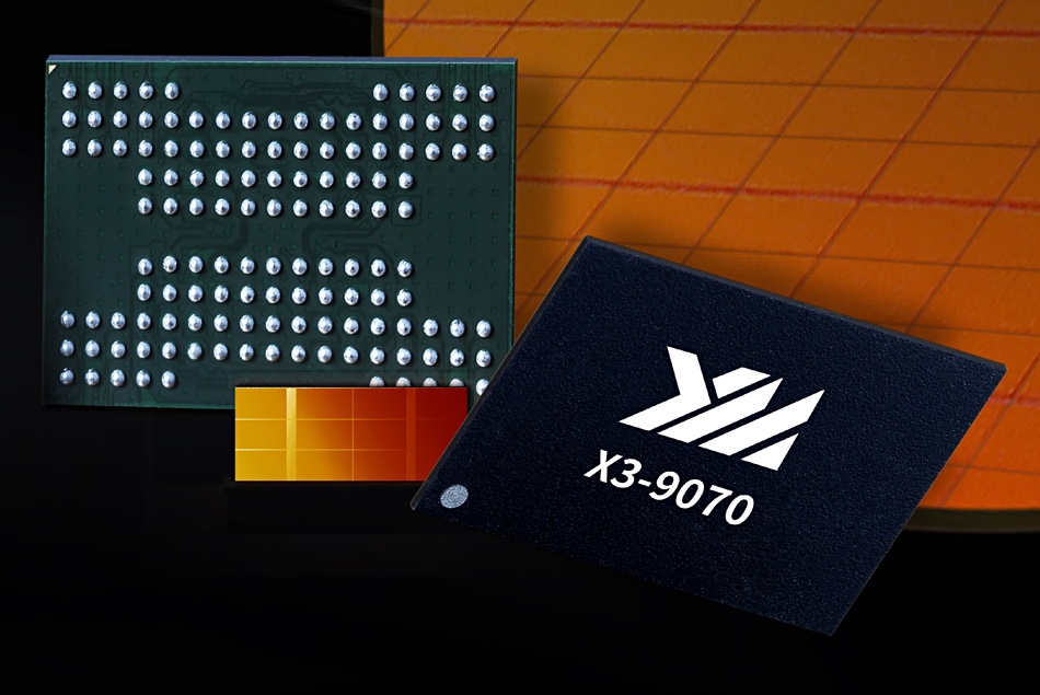
The X3-9070 has a 1Tbit die – the highest density in YMTC’s history, built from 232-layer 3D NAND according to Reuters based on Chinese state-backed media outlet Global Times. YMTC refused to confirm this.
It has a 2,400MT/sec I/O speed – 50 percent more than YMTC’s previous generation of products – while lowering power consumption by up to 25 percent. YMTC is currently shipping and selling 64- and 128-layer products, which presumably used Xtacking v1.0 (64-layer) and Xtacking v2.0 (128-layer) designs.
For example, X2-6070 and X2-9060 products:
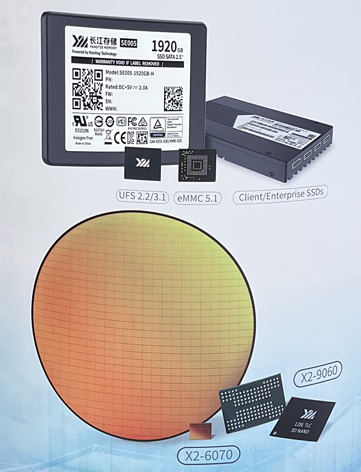
So the XC-9070 has a potential for 25 percent lower power consumption than the X2-9060 SSD.
Xtacking 1.0 delivered 800MT/sec with Xtacking 2.0 doubling this to 1,600MT/sec. YMTC explained in a presentation that Xtacking 3.0 transitioned from a prior Front Side Deep Trench process to a Back Side Source Connect (BSSC) design, which involves a simpler production process and is lower cost.
Version 3 reduces the CMOS die size compared to v2, which allows more NAND planes and features to be supported. The X3-9070 die has six independent planes with asynchronous multi-plane independent (AMPI) operation supported on each plane. This improves both random and sequential IO.
A DRAM-less PCIe 4 x 4-lane SSD design was shown as an example of building an SSD product on the Xtacking v3.0 platform;
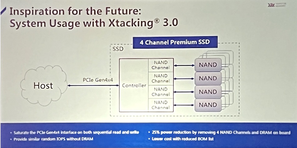
The controller has four channels, each of which links to NAND dies. And the SSD can saturate the PCIe 4 x 4 interface and also can provide the same level of random IOPS as an equivalent (but non-Xtacking) SSD with on-board DRAM.
We have not been provided with any actual IOPS or bandwidth numbers for the X3-9070, nor any data on endurance, capacity options or enclosure format. This leads us to think that it may not be a deliverable product – more of an outline design base on which to develop shippable SSDs.
YMTC booth staff at FMS 2022 were not able to answer any detailed questions at all or even simple ones, such as the X3-9070’s layer count. Such secrecy inevitably raises doubt about the status of the product.
An add-on to the US CHIPS Act prevents suppliers shipping technology to China enabling its companies to build 128-layer or greater 3D NAND. YMTC has said it’s building a second NAND fab and its fitting out could be affected by this restriction.


