Commvault has continued its revenue growth trend with a massive rise in profits in its first FY2022 quarter. This was the company’s fifth successive growth quarter.
Update. 28 July 2021. Earnings call information added and clarified Metallic customer count doubling.
Revenues for the quarter ended June 320 were $183.4 million — a rise of six per cent year-on-year — with profits of $13.9 million. That’s up 504 per cent, which is, to say the least, quite a rise. In fact it was Commvault’s largest profit for at least the past 24 quarters — our records don’t go any further back.
Sanjay Mirchandani.
President and CEO Sanjay Mirchandani said: “We are pleased that the momentum from the prior fiscal year continued into our first quarter. We remain confident that our transformation has put us in position to thrive in a post-pandemic world.”
Financial summary:
Total recurring revenue — $142.2M, up just one per cent year-on-year;
Annualised recurring revenue — $532.8M at quarter end, up seven per cent;
SW and products revenue in quarter — $82.3M, up 35 per cent;
Services revenue in the quarter — $101.3M, up five per cent;
Free cash flow — $35.8M, compared to $13.6M a year ago;
Gross margin — 86.9 per cent vs 86.2 per cent a year ago;
Earnings per share — $0.62 compared to $0.51 a year ago;
Total cash and investments — $359M vs $397M in the prior quarter.
Commvault has moved to a subscription business model and the total recurring revenue of $142.2 million represented 78 per cent of total revenue. The rise in software and products revenue was driven by a 23 per cent increase in revenue from portfolio deals (deals less than $0.1 million in software and products revenue).
Larger deal revenue (deals with greater than $1 million in software and products revenue) represented 69 per cent of Commvault’s software and products revenue in the quarter. The number of large deal transactions grew 34 per cent year-over-year to 185, and the average dollar amount was approximately $305,000.
Wells Fargo analyst Aaron Rakers told subscribers this was “down from $313K and an estimated $402K in the prior and year ago quarters, respectively.” However, Commvault booked its largest ever subscription software deal in the company’s history a year ago, making the year-on-year comparison difficult.
There were more than 300 new Metallic (Backup via SaaS) customers in the quarter, with more than half of them new to Commvault. More than half of the Metallic customers use other Commvault products and more than a quarter of them have two or more Metallic services.
In the earnings call Mirchandani said: “We’re also seeing continued adoption among enterprise customers with greater than $100,000 in Metallic ARR. The number of these customers nearly doubled this past quarter. … it’s a rising star in our portfolio. … we’re very pleased with where we’re going with this.”
The outlook for next quarter is for revenues of $184.5 million — a 7.8 per cent year-on-year increase. CFO Brian Carolan pointed out that: “Q2 is … typically a challenging quarter from a seasonality perspective.”
File and object data migrator Datadobi has updated the underlying software engine used by its DobiMigrate and DobiProtect products, making it faster and more reliable.
DobiMigrate moves file and object data between multiple on-premises vendors’ products and multiple public clouds. DobiProtect creates a golden and immutable copy of file and object data on any vendor’s NAS filer or in the public cloud as a protection against ransomware.
Carl D’Halluin, Datadobi’s CTO, provided an announcement quote, saying: “The scale and complexity of unstructured data in today’s heterogenous storage environments have proven to be quite a challenge for organisations … “Datadobi’s engine enables customers and partners alike to gain control of and utilise their unstructured data across environments on-premises and in the cloud.”
Version 5.12 of the software engine has two main additions. First, the NFS and SMB file access layers in the engine have been re-architected for data copying and filesystem integrity verification in multi-vendor environments. There are low-level NFS and SMB stack optimisations for data and metadata, smart protocol communication pipelining, and Datadobi has parallelised the file access workloads over multiple servers.
That should make moving data faster and scaling better. In fact Datadobi claims the engine’s data copy and verification speed is now far ahead of any competing product.
Second, Datadobi claims a patent-pending chain of custody technology allows detailed reasoning about data and metadata semantic equality during a data copy job, eliminating inter-vendor incompatibilities and vendor-specific behaviour during multi-protocol migrations. This increases the data and metadata integrity preservation during the data move.
Semantic equivalence or equality means that two data elements from different sources (vocabularies) have data with similar meaning — through class or concept equivalence, property or attribute equivalence, or instance equivalence.
Layered engine
The v5.12 engine has five layers:
Orchestration — automated data mobility and protection processes.
Insights and Intelligence — scanning and reporting technology into an entire unstructured data lake, discovering how data is distributed over servers and cost centres.
Integrity Enforcement Technology — data verification, data read-back, chain of custody, and fine-grained data and metadata integrity levels.
Interoperability — connectivity with other vendor’s storage products and the public clouds.
Scan and Copy.
The software is available now and Datadobi says it will support a roadmap of coming new features.
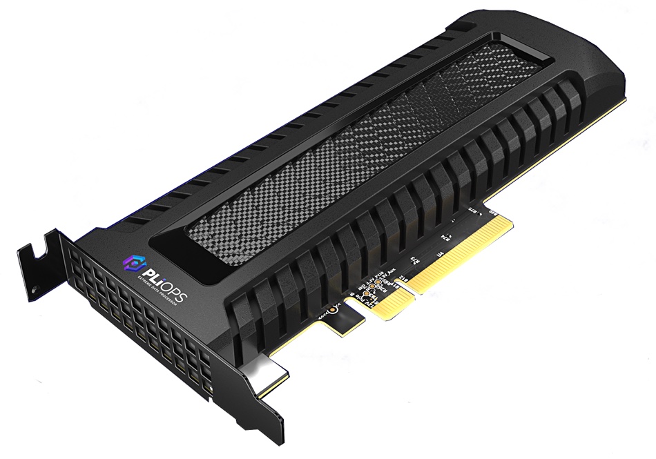
Israel-based startup Pliops has unveiled its Extreme Data Processor (XDP) storage processor product to offload server X86 CPUs and accelerate data-intensive apps with better-designed processor resources.
Pliops — pronounced Ply-Ops and meaning more IOPS — has been developing its XDP storage processor since 2017, reasoning that X86 processors are getting drowned by the increasing demands of relational, NoSQL and in-memory databases, analytics, AI/ML, 5G, and IoT applications — all of which need lots of data-handling processing.
Uri Beitler, Pliops co-founder and CEO, provided context in a statement: “The data needs of today and tomorrow are not compatible with the data centre architecture of yesterday. As data grows exponentially, our ability to handle the data must grow too. What’s needed is a revolutionary data processor – one that doesn’t take a revolution to deploy at scale.”
The XDP is a specially-designed low-profile, PCIe bus-attached accelerator sitting between NVMe SSDs and data-requesting applications. It provides up to 3.2 million random read and 1.2 million random write IOPS and can store up to 128TB of data on 64TB of SSDs.
Pliops low-profile, AIC format XDP.
The card supports QLC (4 bits/cell) flash and can make it perform like more expensive TLC (3 bits/cell) NAND, with TLC endurance levels. It supports all data centre SSDs, atomic database writes and features a block or a key:value (KV) interface.
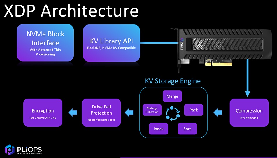
Key:Value store engine
There is a KV library API that is compatible with RocksDB and the NVMe-KV standard.
The XDP’s KV storage engine (RocksDB-on-a-chip, so to speak) works with relational databases (MongoDB, MySQL, Oracle, etc), NoSQL databases (Redis, Aerospike, Hbase, etc), analytics apps (elastic, spark, Splunk and Hadoop) and software-defined storage products like Ceph, MinIO and Nutanix and other object storage. Pliops tells us that block IO, when compressed, appears as variable-sized KV data. It also says that the XDP is binary-compatible with RocksDB.
Pliops XDP architecture graphic.
In general, Pliops claims its XDP ensures KV stores achieve an order of magnitude increase in price/performance and scaling. For Redis it can provide sub-millisecond data access latencies and DRAM-like IOPs from SSDs, although no DRAM caching is used. The card can provide an up 2x increase in read bandwidth and 3x to 4x improvement in write bandwidth for a server.
Performance booster
Pliops says the XDP card can provide an overall 10x performance gains for databases, analytics, and AI/ML work. The product provides on-board compression, thin provisioning, and both data and write reduction with up to 6x space savings increase and protects against drive failure with its RAID-like DFP (Drive Fail Protection) feature. DFP can rebuild a failed 7TB SSD in 35 minutes.
Because it enables fewer servers to do more application work, Pliops estimates the XDP can provide an up to 5x cost saving on data centre infrastructure.
In other words, a Pliops-assisted environment needs fewer servers and fewer and cheaper SSDs to achieve a given level of performance, driving down cost or increasing performance. Possibly even both.
Pliops has existing customers and is basing its claims on their experiences:
$100B US-based Pure SaaS Provider for database application for core service;
Top 3 China Hyperscaler to enable QLC and ultra high node level reliability for EBS;
Top Semiconductor Manufacturer to for validation and manufacturing quality data in MySQL, Mongo, Redis, ML;
US Government HPC Lab for file system and multiple native KV applications.
Download an XDP white paper here (registration required).
Pliops’s XDP is available from multiple distributors and server OEMs, and the company is expending its go-to-market and product development functions. Its customers are going to be enterprises and MSPs.
Comment
The XDP is a storage-specific accelerator card and, as such, is part of the general data processing unit (DPU) technology area. It is rather like a super-SmartNIC because it does more than act as an intelligent network interface card. If we consider an external storage array to be a block interface, dual-X86 controller device presenting a mass of storage drives to servers as a single resource then Pliops’s XDP replaces the storage controller.
It has rough similarities to Fungible’s FS1600 and Nebulon’s original and cloud-managed Storage Processing Unit card. This Nebulon SPU has since evolved into smartEdge and smartCore products, delivering self-service infrastructure provisioning, infrastructure management-as-a-service, and enterprise shared and local data services.
The Fungible FS1600 is a self-contained 2U 24-slot storage server using NVMe SSDs and a pair of Fungible F1 controller chips. In contrast, the XDP is an add-in card (AIC) to an existing server.
President Steve Fingerhut said in a briefing: “We could work with Nebulon. We want to be a building block supplier and work with everybody … We don’t have storage array partners.” Our impression was that we should watch this space.
PIiops company timeline
May 2017 — Founded by CEO Uri Beitler, Chairman Aryeh Mergi and CTO Moshe Twitto.
Start it, build it, sell it — Aryeh Mergi was previously a founder at M-Systems (bought by SanDisk), ActivePath (bought by Broadridge) and XtremIO (bought by EMC).
Pliops’s investors include Intel Capital, Xylinx, Western Digital, Nvidia and Softbank.
Infinidat’s Infinibox arrays have been integrated with ServiceNow’s ITOM Visibility so they can show up and be managed within ServiceNow’s IT estate operations.
ServiceNow provides IT systems management as-a-service and is widely used across businesses, boasting more than 4000 customers. Its latest release uses AI technology to help fix problems in a customer’s IT estate. IT Operations Management (ITOM) Visibility is a suite of ServiceNow offerings including Discovery, Service Mapping, Certificate Inventory and Management, Graph Connectors, Configuration Management Database (CMDB), Firewall Audits and Reporting.
Erik Kaulberg, Infinidat’s VP for cloud and business alliances, said: “Our integration with ServiceNow is a natural extension of Infinidat’s multi-pronged AIOps strategy … We’ve heard a clear need for this integration from large mutual customers, and our … InfiniBox API coupled with ServiceNow’s extensible Discovery Patterns approach made it easy to get it done.”
Infinidat says the integration extends ServiceNow’s out-of-the-box Discovery capabilities to provide visibility into InfiniBox systems, broadening Infinidat’s ecosystem of multi-vendor AIOps capabilities for large-scale enterprise and service provider environments. Discovery can detect and understand all components of Infinidat’s storage systems and add them to the ServiceNow CMDB.
It automatically builds dependency relationships between the InfiniBox systems and components, host systems, and attached networks. The CMDB inclusion forms a foundation for event correlation, log analysis, and other capabilities in ServiceNow’s product suite. This means ServiceNow AIOps systems and workflows include Infinibox arrays in the data infrastructure for which they provide centralised monitoring.
It also means Infinidat customers can use ServiceNow Service Mapping to understand what services are powered by InfiniBox and build migration plans when becoming InfiniBox customers.
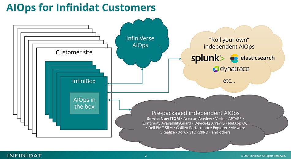
Kaulberg told us there are three aspects to Infinidat’s AIOps features:
In-house InfiniVerse AIOps;
Roll-you-own, general purpose analytics — elasticsearch, Dynatrace, Splunk, etc.;
Pre-packaged independent AIOps — Arxscan, Continuity, Dell EMC SRM, Device42, Galileo, NetApp OCI,Veritas APTARE, VMware vRealize, Xorux and more.
Kaulberg said that there is “a very broad and level AIOps playing field … with no clear winner”. In his view Infinidat “really does have presence across all three of the AIOps areas: in-house, roll-your-own, and pre-packed offerings. He said: “We’ve invested before the market consolidates in AIOps.”
Kaulberg suggests AppDynamics is a level above such infrastructure players, and Infinidat would plug in via an intermediary.
Availability
The updated Discovery and Service Mapping software options with the Infinidat integration are available immediately for download from the ServiceNow Store. Each discovered InfiniBox requires four ServiceNow Discovery Subscription Units, available from ServiceNow representatives.
General AIOps support
Infinidat recently said it had a strong AIOps momentum and we suggested it didn’t have much third-party AIOps support. We were wrong.
In fact AIOps is now provided by an ecosystem of third parties, not just a few specialised suppliers such as AppDynamics and Virtana.
Infinidat lists a plethora of suppliers with which it has links: Arxscan, Continuity Software, elastic, Device24 Array IO, Galileo Suite, Splunk, VMware, Veritas and Xorux plus others.
The intention is that Infinidat will fit in with its customers’ preferred AIOps approaches.
PROMO 2020 was an impactful year for file storage. Almost overnight, companies were forced to rethink how they manage, access and derive value from data, casting a bright light on the advantages of cloud-based technologies. After navigating unforeseen business challenges, including ransomware attacks, remote work environments, and more, it is time to discover how to apply those lessons learned.
A broader shift to the cloud coupled with an explosion of unstructured data is driving an increasing realisation that managing and extracting value from your data is critical to digital transformation. There’s also the fear that disruption and downtime can seriously imperil your company’s future, whether that’s due to creaking traditional file infrastructures or ever more aggressive attacks from ransomware extortionists and other criminals.
Which is why you should register – for free – for Nasuni CloudBound21, a global online event being hosted by Nasuni, a leading provider of cloud file storage. Nasuni CloudBound21 is dedicated to providing IT leaders with the resources and practical skills required for their organization to thrive in today’s world of modern file storage.
Nasuni CloudBound21 runs September 28th-30th with a jam-packed agenda including powerful keynote speakers, innovative sessions, and networking opportunities designed to equip attendees with tangible takeaways during a time zone that best matches your availability.
Learn from peers, industry experts, and Nasuni customers alike as they share practical insights, real-world case studies, and best practices.
Naturally, you’ll get up to speed on the latest technology and thinking in data protection, file backup, ransomware, and cloud-based solutions, courtesy of Nasuni who services companies such as Pernod Ricard, SDL and Vossing. You’ll also hear how your file storage strategy underpins and interacts with other key issues, such as digital transformation, cloud migration, and the cloud ecosystem. Each day features four hours of content, meaning you can benefit from all this knowledge, and still get on with your day job.
You’ll learn how you can potentially realise massive cost savings on your file management and storage. And you’ll hear from real world companies who have done just that. Plus, you’ll get exclusive updates on upcoming Nasuni features.
The challenges of managing your corporate data are not going to go away. But by heading here and registering for Nasuni CloudBound21 you’ll be better equipped to tackle them head on.
The bankrupt Tsinghua Unigroup is looking for a strategic investor or group to pump in ¥500 million ($77M) to its bank account as the first step in clearing its debts.
Tsinghua’s total liabilities exceed ¥200 billion ($30.8B), according to a statement it posted on China’s National Enterprise Bankruptcy Information Disclosure Platform (NEBIDP) web site. It needs to be rescued by a wealthy entity with the overall semiconductor, networking and cloud industry experience required to sort out an over-stretched and loss-making group with more than 286 subsidiaries.
The longed-for rescuer must be worth more than ¥50 billion ($37.7B) in minimum total assets, or have at least $3.1 billion in net assets, and put in a bid by September 15. All this is reported in the South China Morning Post.
Tsinghua trashes itself
Tsinghua’s nearness to bankruptcy was revealed earlier this month, when the Hong Kong-listed Huishang Bank went to court to start bankruptcy proceedings over bond debt it was owed by Tsinghua. Subsequently Tsinghua, also known as the Zinguang or Unisplendour group, posted the NEBIDP document stating its financial position.
According to this posting, the group apparently used capital from bond issues to buy a string of other companies in the six years following 2013:
2013 — Spreadtrum for $1.78 billion;
2013 — RDA for $910 million;
2015 — 51 per cent stake in H3C for $2.5 billion;
Investment in Western Digital — $3.8 billion.
Tsinghua has also invested heavily in building semiconductor plants:
Wuhan projects — $24 billion;
Chengdu storage project — $24 billion;
Nanjing Integrated Circuit Base (phase 1) — $10.5 billion;
Guangzhou chip fab — $154 billion.
The income from its acquisitions couldn’t match the group’s spending commitments, so it started failing to make bond interest payments, triggering the Huishang Bank court action. Trading of six of Tsinghua’s onshore bonds stopped on July 21.
Comment
A Tsinghua Group bankruptcy restructuring exercise could be a good match with the interests and capabilities of the Bain Group, which is heavily involved in the restructuring of the Toshiba Memory Business — now called Kioxia. But would any non-Chinese investing entity be interested in rescuing a Chinese chip-making group involved in China’s march to semiconductor self-sufficiency?
How would the US government view such a course of action by a US-led investment group — particularly with China identified as the source of various hacking actions against US organisations? China’s geopolitical ambitions on the South China Sea have upset neighbouring countries such as Japan, Taiwan and Korea, and it seems unlikely companies there will be interested in helping China become even stronger.
The likelihood is that a Chinese concern — such as Alibaba — will be asked to bid for Tsinghua Unigroup and restructure it into a self-sustaining business.
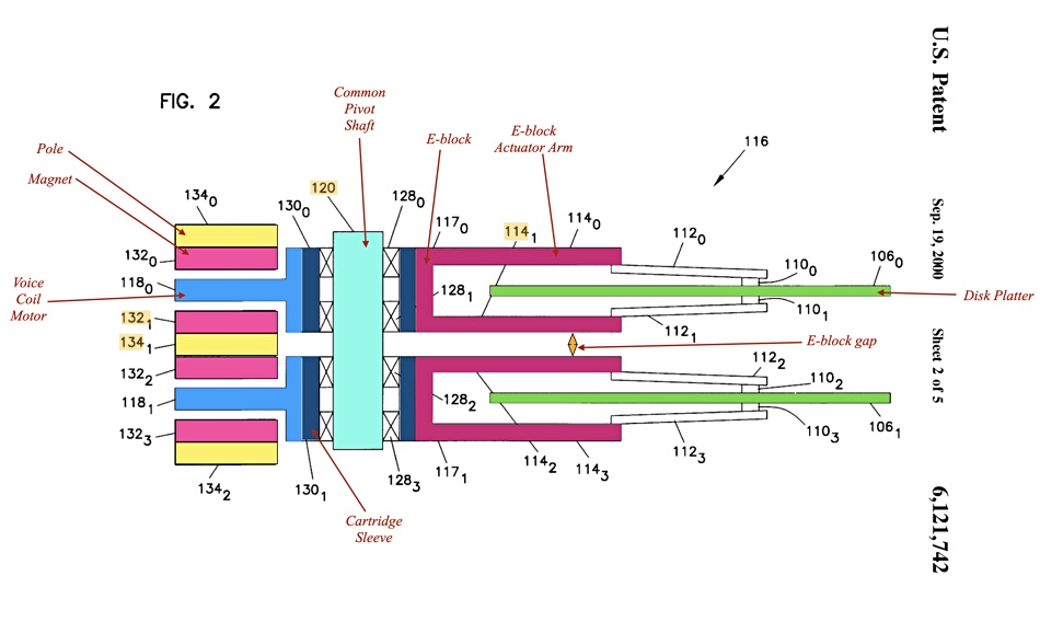
Seagate CEO Dave Mosley hinted at disk drives with more than two actuators in the company’s latest results earnings call. What might that mean, and how might it be implemented?
Currently, Seagate is shipping an Exos 2X14 dual-actuator drive with eight platters and a 14TB capacity. Shipping started in 2019 and, since then, Seagate has introduced 16TB and 18TB single-actuator Exos drives, with 20TB ones on their way. These use a nine-platter design, with the 18TB drive boasting a capacity of 2TB per platter. Should we then expect 16TB, 18TB and eventually 20TB dual-actuator drives?
Actually, no. The additional actuator mechanisms take up space inside the drive enclosure, and capacity has to be sacrificed for that — the second actuator causes a platter space to be used up.
Serial vs parallel
Because Seagate’s Mach.2 dual-actuator tech has two actuators, the big deal is that this doubles the IOPS the drive can sustain and nearly doubles the throughput — a 1.8x to 1.9x increase. The Exos 2X14 increases IOPS from the 80 or so of the single-actuator Exos 14TB drive to around 160, while the throughput on large sequential IO changes from 261MB/sec to about 483MB/sec. How so?
The thing is that, while a drive has multiple platters with a pair of read/write heads per platter (one per surface), nothing — apart from platter spinning and read/write head slider movement — happens in parallel. Only one read/write head can write or read data at a time. A multi-platter spinning disk is a serial device.
A theoretical way to make a multi-platter disk operate in parallel would be have to an actuator per platter — nine actuators for a nine-platter drive. But that would send both the power draw and cost of disk drives higher, and may not be physically possible inside the fixed 3.5-inch drive format.
A look at the drive’s components shows why.
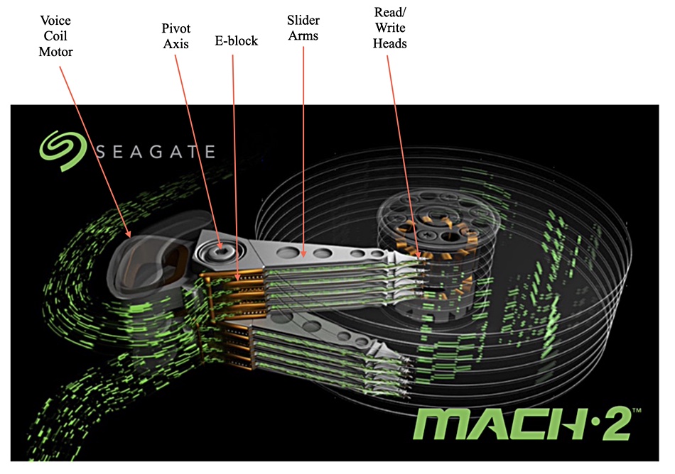
Drive actuator mechanism
All the read/write heads on their slider arms move across the disk’s surfaces by rotating around a shared pivot axis. The sliders are mounted on a single E-block (possibly so called because of its shape). This E-block rotation is caused and controlled by a voice coil motor (VCM), which has an electrically charged coil moving between two magnets on the other side of the pivot from the E-block.
We’ve labelled a Mach.2 image to show these components;
It is obvious after studying Seagate’s Mach.2 image above that there must be two actuators: one for the upper E-block and its slider arms, and a second for the lower E-block. A look at a Seagate patent diagram for a multi-actuator drive shows this clearly.
We have coloured and labelled some components in the diagram to make things more recognisable.
The second actuator needs a second VCM, which increases the component cost and the electricity needed to operate the drive — sending that up by 26 per cent.
The diagram shows a gap between the upper actuator’s VCM and E-block and the lower actuator’s VCM and E-block. This enables them to rotate independently around the pivot axis without touching one another.
Seagate’s Exos 2X14 couldn’t be a 2X18, because the 18TB Exos is a 9-platter drive and the dual actuator mechanism needs space between the upper and lower actuators — labelled E-block gap in the diagram above — and this causes a platter to be lost.
Actuator additions
Knowing this, let’s hypothetically add another actuator, or even two more. Does that mean that we lose a platter per additional actuator?
It could mean that, but we don’t actually know how much of the space needed for a disk platter is actually used up by an additional actuator. It could be all of it, or just some of it — 20 per cent, say. In the eight-platter Exos 2X14, enough of the space is taken up to prevent it being a nine-platter drive.
Therefore, were Seagate to build a dual-actuator drive based on its nine-platter, 18TB Exos product, with a 2TB per platter capacity, the result would be an eight-platter drive with 16TB capacity.
Now let’s add a third and a fourth actuator.
If each one takes up a one-platter space, then a triple-actuator product would be a seven-platter 14TB drive with about 240IOPS and 705MB/sec throughput. The quad-actuator model would be a six-platter 12TB drive with roughly 320 IOPS and 927MB/sec throughput.
The question is whether the gain in IOPS and sequential throughput would be worth the lost capacity, the increased power draw, and component cost.
Suppose each additional actuator takes up half of the platter space, and that four actuators means two platters are lost. Then a quad-actuator drive based on the nine-platter Exos 18TB product would be a seven-platter, 14TB drive. But if each additional actuator took up a third of a platter space, then the quad-actuator product would be an eight-platter drive with 16TB overall capacity.
The E-block gap is a crucial parameter affecting the platter count in a drive with anything more than two actuators.
Logical Unit Number size and component simplicity
The Exos 2X14 is treated by host software as two logical drives, each with 7TB capacity. In effect, there are two 7TB LUNs. If a dual-actuator mechanism was added to the 18TB, nine-platter Exos drive base, the result would be two 8TB logical drives. Adding a triple actuator mechanism that caused two platters to be lost would result in a seven-platter drive with 14TB capacity overall but two unequal logical drives — a four-platter 8TB one and a three-platter 6TB one.
Core multi-actuator drive customers — namely hyperscaler businesses — might be concerned that they then had unequal capacity logical drives.
It may be simpler, from an architectural and component point of view, to double the dual-actuator drive mechanism to get a quad-actuator drive stack — if the four actuators in total only caused the sacrifice of a single platter. That way you would get minimal lost capacity and maximal increase in IOPS and throughput.
Prognosis
Seagate is not alone in developing this technology. Western Digital demonstrated multi-actuator technology at the OCP summit in March 2019.
Together with Seagate hinting at having more than two actuators, Blocks & Files thinks that the HDD industry — Seagate and Western Digital certainly and Toshiba maybe — will bring out 16 or 18TB dual-actuator drives by the end of 2022. Seagate may demonstrate a quad-actuator drive by then as well.
This week’s edition of our all-you-can-eat storage buffet has main plates featuring flavoursome Napatech SmartNICs, Scale Computing getting edgy in bed with IBM, Inspur knocking off another benchmark win and Viking/Kalray developing a FlashBox NVME SSD system with DPU acceleration.
There are side plates brimming with tasty finger food, so pick up a napkin and tuck in.
Napatech SmartNICs and radios
SW-defined radio platforms supplier Per Vices Corporation is using Napatech’s programmable Smart Network Interface Cards (SmartNICs) in its Cyan Storage and Playback offering. Applications such as real-time spectrum monitoring and recording require a high-bandwidth, lossless connection between the radio and the storage subsystem in order to ensure the integrity of data captured in real time across a wide spectrum.
Having a high-performance configuration for spectrum monitoring and recording brings benefits for use cases such as signal interception, spectrum policy enforcement, interference detection and the monitoring of restricted areas such as prisons, military facilities, government buildings and airports.
The Cyan Software-Defined Radio (SDR), which offers up to 16 independent receive chains, each with 1GHz of bandwidth and operation from near DC to 18GHz, must be balanced by the packet capture and monitoring capabilities of the Cyan Storage and Playback system. The Napatech SmartNIC uses four 40Gbps QSFP+ interfaces to the Cyan SDR and delivers:
Capture, monitoring, recording and storage of data at up to 160Gbps;
100 per cent probability of Intercept (POI) across 16GHz of spectrum;
High-performance data processing and higher-capacity storage with no dropped packets;
Application-optimised CPU, GPU and RAM configurations;
Easy integration within larger systems.
Scale Computing and IBM take it to the edge
Edge-focussed Scale Computing is twinning its HC3 appliances with IBM’s Edge Application Manager (EAM) — a management system running on Red Hat OpenShift. EAM enables the deployment, operation and remote management of AI, analytics, and IoT enterprise workloads at edge sites.
Jeff Ready, CEO and co-founder of Scale Computing, said the HC3/EAM infrastructure is “designed to be self-healing and automated, as well as added containerised application management that can help [organisations] grow into the new reality of edge computing.”
IBM’s Evarisitus Mainsah, GM, Hybrid Cloud and Edge Ecosystem, talked about “collaborating with Scale Computing to help clients deploy, operate and manage thousands of endpoints throughout their operations with IBM Edge Application Manager”. The point is to help customers act on “insights closer to where their data is being created, at the edge”.
Inspur racks up another SPC-1 benchmark
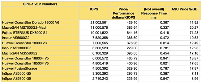
Chinese supplier Inspur said its AS13000G5 distributed, scale-out storage server system achieved an SPC-1 benchmark result of 6,300,529 IOPS and 0.781 ms latency, breaking the world record in distributed storage performance.
SPC-1 measures the ability of a storage system to run input-output operations, measured in calculated SPC-1 IOPS.
The AS13000G5 topped the rankings in single-node performance with a result 68 per cent higher than the runner-up. However it is the sixth highest SPC-1 result in absolute terms:
Top 12 SPC-1 results as at July 2021.
The AS13000G5 uses NVMe SSDs, and can be expanded to 5120 storage units, with IOPS reaching a theoretical 100 million.
Gartner says Inspur ranks in fifth position in global storage sales.
Viking and Kalray’s DPU-driven NVMe all-flash array
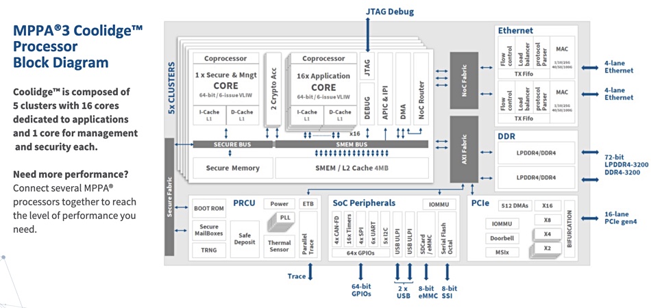
Sanmina’s Viking Enterprise BU and fabless processor developer Kalray are jointly developing a FlashBox array, a JBOF disaggregated storage system using Viking’s VDS2249R chassis and a Kalray K200-LP storage acceleration card based around its MPPA Coolidge DPU (Data Processing Unit).
The MPPA (Massively Parallel Processor Array) DPU is a programmable, data-centric processor and replaces, Kalray says, multiple X86 controller cards. It has up to 80 cores.
MPPA Coolidge diagram.
The MPPA Coolidge DPU is designed, Kalray says, to deliver an unprecedented level of integration, speed and performance at an affordable cost.
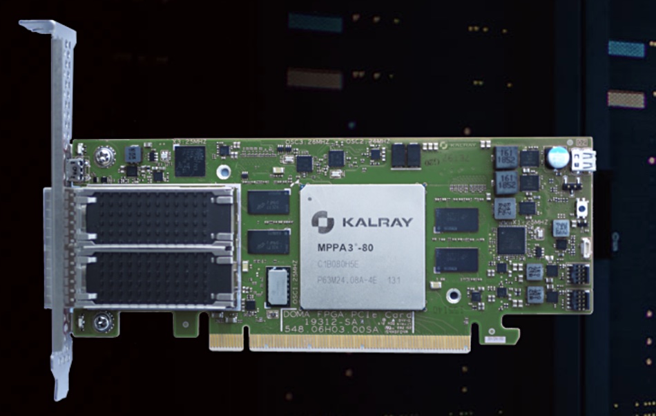
Kalray MPPA Coolidge DPU card.
We have here, Blocks & Files thinks, a French alternative to Pensando. Kalray was founded in 2008 as a spin-off of CEA French lab. Its investors include Alliance Venture (Renault-Nissan-Mitsubishi), Safran, NXP Semiconductors, CEA and Bpifrance.
The FlashBox will be publicly revealed in September. Get a Coolidge DPU product flyer here.
Shorts
Data protector Acronis has integrated its Cyber Protect Cloud with Jamf’s software, a standard in Apple Enterprise Management (AEM). The Jamf Pro application is used by system administrators to configure and automate IT administration tasks for macOS, iOS, iPadOS, and tvOS devices. MSPs can remotely deploy Acronis Cyber Protect Cloud’s range of backup, recovery, and cyber protection services for Apple devices, managing multiple Jamf Pro accounts for multiple instances through a single Acronis account.
This is ingenious. Taiwan-based Chenbro announced a 2U storage server chassis, the RM25324, which accommodates 24x 3.5-inch side access hot-swap hard drives, 7x low profile PCIe slots, and an ATX motherboard, optimised for computing and storage balance to support industrial storage, data centre, and digital surveillance applications. Usually, 24-bay 2U boxes use 2.5-inch drives, and this beast of a box with 3.5-inch disks can store 400TB raw.
Couchbase announced v7.0 of its Couchbase Server database, presenting it as a unified RDBMS+ NoSQL analytics database offering. It processes multi-statement SQL transactions by fusing together transactions and high-volume interactions. Couchbase claims that, for the first time, customers can do multi-document SQL ACID transactions with interactions in microseconds — all within one unified database platform. The company, with 500+ customers, has had its IPO and began trading on July 21.
CrossBar has found a new niche market for its ReRAM (Resistive RAM). It’s being used in hardware security applications with PUF (Physically Unclonable Function) keys as a replacement for SRAM. We’re told that, compared to SRAM, ReRAM-based PUF cryptographic key technology has a higher level of randomness, much lower bit error rate, resists invasive attacks, and has the capability of handling a broad range of environmental variations without requiring fuzzy extractors, helper data or heavy error correction code.
NBC Olympics, part of the NBS Sports Group, is using petabytes of Dell EMC PowerScale storage system capacity to store video captured at two production locations for the Olympic Games in Tokyo for sharing with USA viewers.
Dell Technologies commissioned Forrester Research to conduct a Total Economic Impact (TEI) study to examine the benefits, costs and risks enterprises encounter when deciding to invest in as-a-Service. Dell’s APEX Data Storage Services helped the customers in the Forrester TEI study:
Eliminate costs of over-provisioning, reducing storage costs by 20 to 45 per cent;
Save as much as 50 per cent in IT time;
Accelerate deployment time of storage by as much as 86 per cent.
Data lake analytics developer Dremio announced a cloud-native SQL-based data lakehouse service, Dremio Cloud, saying it enables organisations of any size to leverage a no-copy open data architecture that eliminates the need to copy data into expensive and proprietary data warehouses. An automatic onboarding option establishes the necessary connection to the user’s AWS account, allowing data consumers to connect via their favourite tools and start querying data instantly.
Cloud-native archiver FalconStor announced the pricing of an underwritten registered public offering of 285,000 newly issued shares of its common stock at a public offering price of $4.10 per share, for total gross proceeds of approximately $1.16 million. It will use the cash to expand marketing and distribution, ongoing product development programs, finance potential acquisitions of complementary businesses, and for working capital and general corporate purposes.
Veeam’s Kasten business unit announced its Kubernetes-focussed K10 data management software is now available through the Red Hat Marketplace.
Microchip Technology today announced the Adaptec Smart Storage PCIe Gen-4 NVMe Tri-Mode SmartRAID 3200 RAID Adapters, and SmartHBA 2200 and HBA 1200 Host Bus Adapters. These adapters enable NVMe and 24G SAS connectivity and manageability. They deliver between 8 and 32 ports of NVMe 4.0 and/or 24G SAS drive support, and offer both 8x and 16x PCIe Gen-4 CPU interface options and up to a 4x performance improvement over previous generations.
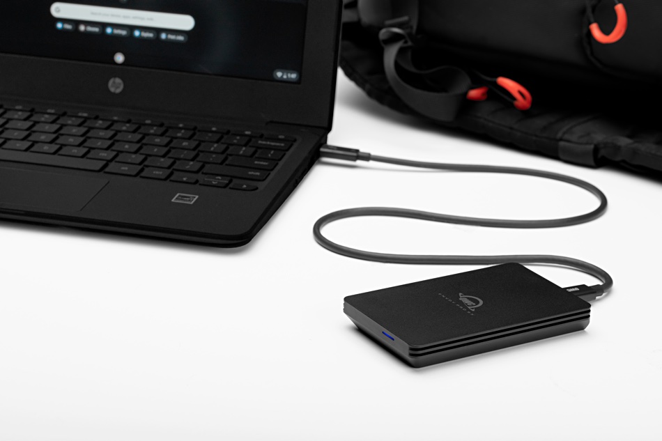
OWC has announced its Envoy Pro SX Thunderbolt portable SSD, saying it offers the fastest and most reliable performance available in a portable drive. It’s certified dust-proof, drop-proof, and waterproof, and provides up to 2,847MBps. 240GB to 2TB models are available now, starting at $199 on MacSales.com.
OWC Envoy Pro SX.
PNY has announced ultra-high-endurance LX2030 and LX3030 SSDs for Chia plotting. They are M.2 drives with an NVMe PCIe Gen-3 interface. The 2TB LX3030 has a Chia plotting TBW rating of up to 54,000. A 1TB LX3030 can create 2PB of plots before wearing out — 27,000TBW. A 2TB LX2030 sustains 10,000TBW.
Pure Storage announced FlashStack as-a-Service, having flagged its intentions in November last year. FlashStack is a reference architecture converged system using Pure flash storage with Cisco servers and networking. It’s also adding Portworx Cloud Consumption to allow customers’ consumption of Portworx (consumed hours) to match the ebbs and flows of their applications instead of buying specific Portworx licences per server.
NAS supplier QNAP has signed up Tech Data as a distributor in the UK.
Quobyte, which produces unified block, file and object storage for high-performance computing and machine learning, announced it has a native HDFS driver. This implements and replaces the HDFS API. Applications talk to Quobyte instead of HDFS, but won’t notice the difference.
Logic meets magic — Spectra Logic is partnering StorMagic to produce an end-to-end active archive for video surveillance and digital evidence management. StorMagic is contributing its ARQvault, a data-mover and intelligent repository using analytics to manage and retrieve digital assets. These assets will be stored in Spectra Logic’s BlackPearl NAS system and tape libraries.
Storage Made Easy (SME) announced an SMBStream product ,which accelerates access to SMB shares over the internet. A small agent is co-located in the same network as the NAS or Filer providing the SMB Share, providing access to a containerised controller at a remote site via a TLS 1.3-encrypted tunnel. SMB acceleration is a factor of 10x faster than a typical VPN, and is tolerant of high latency and dropped packets. SMBStream is filer-agnostic and compatible with on-premise NAS or Windows Filer shares, or in-cloud SMB shares such as Amazon FSx or Azure Files.
Chinese supplier TerraMaster has a D16 Thunderbolt 3 compact 16-bay tower storage product with Thunderbolt 3 interface and up to 40Gbps data transfer speed. This is suitable for 4K/8K video editing. Equipped with a pair of Thunderbolt 3 40Gbps ports and a professional-grade RAID controller, the D16 Thunderbolt 3 delivers speeds of up to 2,817MBps when fitted with 16 SSDs in RAID 0 array mode on Windows. In RAID 6 mode, the storage device can deliver speeds of up to 2,480MBps.
TerraMaster D16.
TerraMaster also announced a F4-421 4-bay professional NAS powered by an Intel quad-core processor with dual Gigabit network ports for improved networking reliability. It supports network aggregation and failover with dual LAN ports, automatically switching to the second networking port in cases of downtime.
Data protector Veeam said its annual recurring revenue increased by 26 per cent year-over-year in the second 2021 quarter — its 14th consecutive quarter of double digit growth. Later this year it will release cloud-native offerings for AWS, Azure, Google Cloud, Office 365 and the first integration of Kasten K10 for Kubernetes into the Veeam Platform.
Microfocus’s Vertica analytics platform has reached version 11, delivering support for Docker containers and Kubernetes, machine learning and time series capabilities, and Eon Mode in Azure. Vertica claims it is a unified analytics platform with the fastest performance at unlimited scale.
Virtium announced second-generation StorFly Series3 M.2 NVMe SSDs supporting PCIe Gen-4. They are DRAM-less, have up to 2TB capacity, use 3D TLC NAND, and support industrial temperatures of -40°C to 85°C as well as ruggedization options for extreme environments.
Virtuozzohas bought OnApp. The resulting system stack for CSPs, MSPS and hosting providers will pair Virtuozzo’s virtualization, containerization, storage and orchestration capabilities with features of OnApp’s self-service management platform.
Votiro can sanitize files coming from AWS storage with its Secure File Gateway and an S3 bucket connector. It disarms the file of any malware, creating a completely safe version. After the file has been processed, it is returned to the S3 bucket — replacing the original file with the tagged, cleaned file — and safe for users to open, save, edit, and share without risk.
Winbond x8 Octal interface NAND can provide cost effective embedded code storage in high density and in the same form factor as NOR Flash. It’s announced interoperability with Synopsys’s DesignWare Synchronous Serial Interface (SSI) IP, which offers high transfer rates and low latency. Together they deliver a NAND flash memory product for automotive, mobile and IoT SoCs.
On-premises storage array service provider Zadara announced that Africa’s largest network of interconnected, carrier- and cloud-neutral data centre facilities has added Zadara’s edge cloud services to its marketplace. Africa Data Centres (ADC) gives customers in its facilities access to fully managed IT infrastructure on demand. Zadara’s products and services are currently available in Midrand, South Africa, and will soon be expanded into all 16 ADC locations throughout the continent.
Less than a year after emerging from stealth, Kubernetes data-moving startup Ionir has a new CEO.
Ionir was created from the ashes of Reduxio and uses the latter’s Magellan data state capture technology in its software. Incumbent CEO and co-founder Jacob Cherian has moved into a newly-created Chief Product Officer role with exec chairman Mike Wall taking on the CEO responsibility.
A Wall statement explained: “Kubernetes and containerisation together redefine cloud and IT infrastructure, freeing applications to run anywhere. However, the data gravity challenge must be overcome to ensure true application agility. Ionir is the only technology that addresses the data challenges of running Kubernetes at scale. This level of system-wide disruption creates gigantic market opportunity.”
Mike Wall, CEO, Ionir.
Wall was previously the CEO and chairman of object storage supplier Amplidata, which was bought by Western Digital’s Hitachi GST business unit in 2015.
In previous roles he was Atempo CEO before selling the company to ASG, and GM of Intel’s Storage Division. If we go by precedent then, Wall will grow Ionir’s business and sell the company.
Ionir says it is growing rapidly in North America — a claim backed up by investor Jerusalem Venture Partners general partner Fiona Darmon. The expansion is boosted by the launch of its Continuous Integration/Continuous Delivery (CI/CD) pipeline acceleration offering. This is the near-instant cloning of time-stamped data copies that can be used at any point in an application development cycle, thus accelerating it according to Ionir.
Call us insensitive for asking, but, if the company is doing so well, why does it need a new CEO?
Although it is relatively early days in the general enterprise adoption of Kubernetes-orchestrated containers, the size of the storage and data services opportunity is vast, with both startup and incumbent suppliers piling in to the market. Dell (Project Karavi), NetApp (Astra), HPE (Ezmeral), Pure Storage (Portworx), Red Hat, Suse Rancher and Veeam (Kasten) are some of the mainstream suppliers involved while MayaData, Robin.io and StorageOS are three of the startups.
Ionir has developed differentiated marketing but, like everyone else, is facing intense competition. Having the best technology for aspects of Kubernetes data services, as it says it has, may not be enough when marketing impetus, partnerships, and channel forces are added in to the business success mix. Time is of the essence here, as we are seeing a Kubernetes storage/data services land grab and all available niches will be staked out soon enough
Wall provided Amplidata with a good exit in the object storage market, and did well for Atempo in the data protection market. Atempo had its own Miria data-moving technology. Perhaps Wall thinks he can use his Amplidata and Atempo commercial experience to propel Ionir into a higher level of growth and gain ground compared to the other startups.
GigaOm positions Ionir as a non-enterprise Kubernetes storage supplier, and that may be something Wall will want to change. Ionir wants its share of the gigantic opportunity Wall is seeing, and he aims to make sure what Ionir wants Ionir gets.
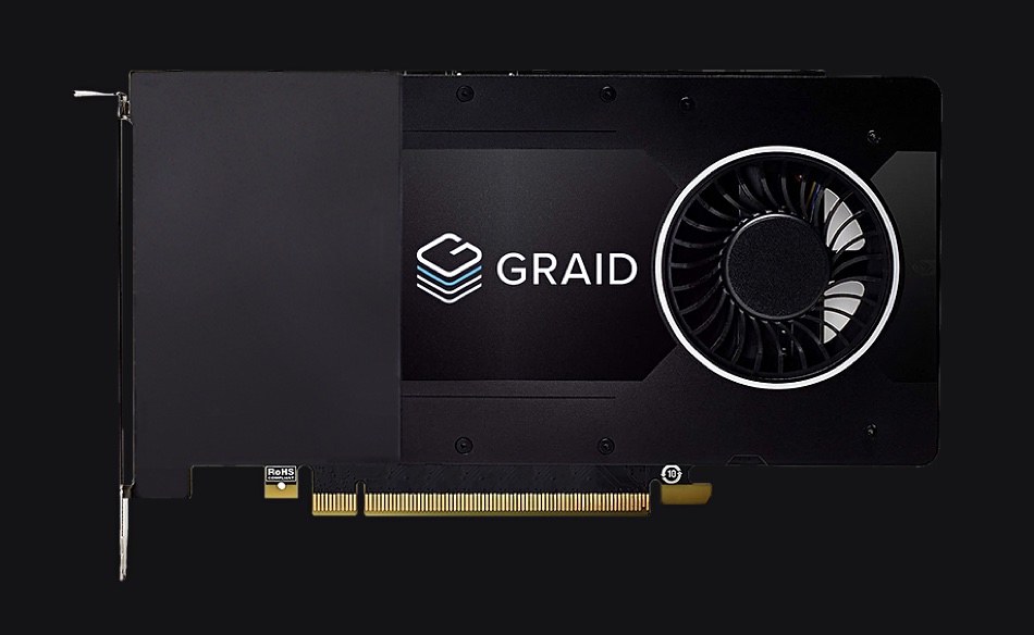
Startup GRAID has designed a RAID card using a massively multi-core processor designed for AI, and says it can keep up with NVMe SSDs without sucking up host server CPU cycles.
Traditional RAID cards use an application-specific integrated circuit (ASIC) and can handle SAS and SATA disk drives pumping out 200 IOPS and around 150MB/sec of throughput, according to GRAID documentation. They also live in the data path. But an NVMe SSD can produce a million IOPS and up to 7GB/sec of throughput which more than saturates a disk drive-era RAID card.
The AI chip on GRAID’s SupremeRAID card carries out all the RAID calculations, offloading the host CPU in the same way as a SmartNIC. There is no DRAM cache on the card, hence no need for a battery backup system. As the SSDs are PCIe-connected they can be in U.2, M.2 or Add-in-Card formats — and there can be up to 32 of them per card. The RAID calculations are done out-of-band. (The card also supports SAS and SATA SSDs, although the fabric access is then not possible.)
GRAID Supreme RAID card.
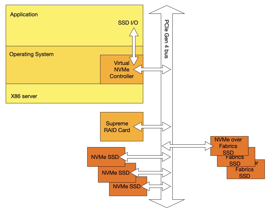
We still need RAID to cope with SSD failure, and software RAID needs server CPU cycles. What GRAID has done is to build a supercharged RAID hardware card — its SupremeRAID SR-1000 — along with virtual NVME controller software, and hook the two up using the PCIe bus. Gen-3 and -4 PCIe buses are supported.
NVMe SSDs also hook up to the PCIe bus and there is no need for links between disk drives or SSDs and the RAID card. This design also means that the SSDs can be remote from the server and accessed across an NVMe-over-Fabrics set up.
GRAID SupremeRAID diagram created by Blocks & Files.
GRAID says this is the first NVMe SSD RAID system that can also protect SSDs connected by NVMe-oF.
Supported host server operating systems are all Linux — CentOS 8.3, RHEL 8.4, Ubuntu 20.04, openSUSE Leap 15.2, and SLES 15 SP2. The card’s software is extensible and, for example, data reduction calculations could be added. The card can also play a role in composable systems — contributing NVMe-oF-accessed SSDs from a remote JBOF to a composed server.
The card’s RAID-5 performance is 6.4 million random read IOPS and 765,000 random write IOPS. Sequential throughput is 92GiB/sec reading and 10GiB/s writing — it’s massively skewed to reading. RAID-10 throughput is 100 GiB/s reading and 33GiB/s writing. (1GiB = 1.07374GB.)
A Gigabyte R282-Z94 gen-2 AMD server fitted with a PCIe gen-4 bus and 20x Kioxia CM6-R SSDs went even faster: 1.4 million random read IOPS, 350,00 random write IOPS, 6.9GB/sec sequential reads, and 4.2GB/sec sequential writes. PCIe gen-4 buses make servers fly.
Background note
GRAID Technology is headquartered in Silicon Valley, with offices in Santa Clara and Ontario, California and an R&D centre in Taipei, Taiwan. It was founded in 2020 by CEO Leander Yu and the funding status is unknown.
An end-user survey by research firm Coldago finds users highly positive about the public cloud, cloud-native development, and all-flash arrays, with some surprising vendor rankings concerning Infinidat, VAST Data and Silk.
The End-Users Survey 2021 looks at storage and data management technologies, products, projects and processes. It also identifies end-users’ needs, perceptions and adoptions. The survey looked at 1347 US companies and 712 European ones — in the UK, Germany and France. Half the surveyed users were from enterprises and the other half from small and medium business.
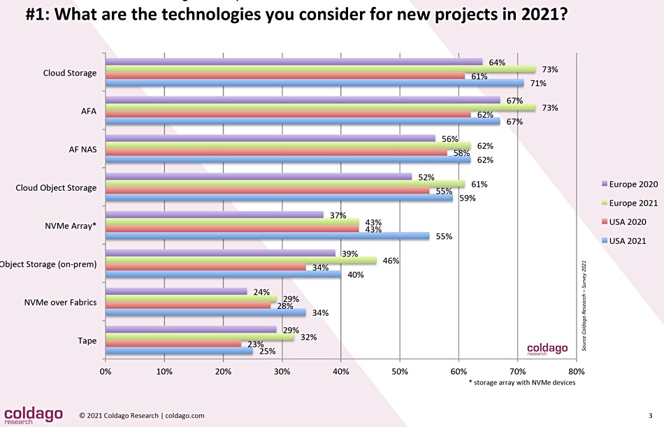
The report is a series of charts and the first one looks at storage technologies considered for new projects in 2021:
Each of the technologies shown has Europe 2020 and 2021 results followed by USA 2020 and 2021 results, so we can note the trends. They are ordered by the USA 2021 percentages. Cloud storage is the top technology, followed by all-flash arrays (AFA) and all-flash NAS. Somewhat surprisingly, tape technology is in the list, only slightly behind NVMe-over-Fabrics.
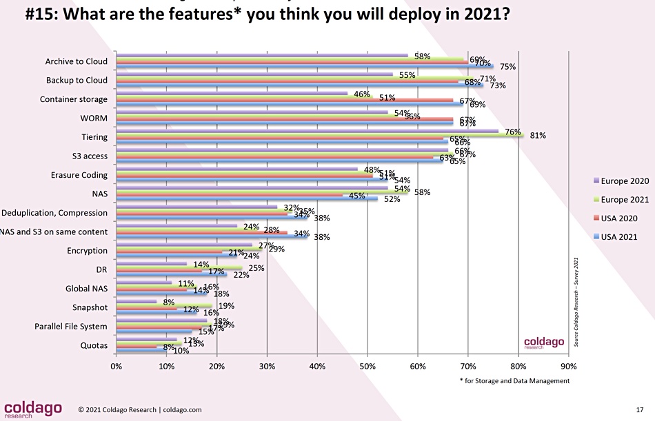
The specific features considered for 2021 deployment are:
Archive and backup to the cloud are the top two, with container storage in third place. Looking down the list it’s apparent that parallel file systems are the equivalent of a minority sport, coming in at number 15.
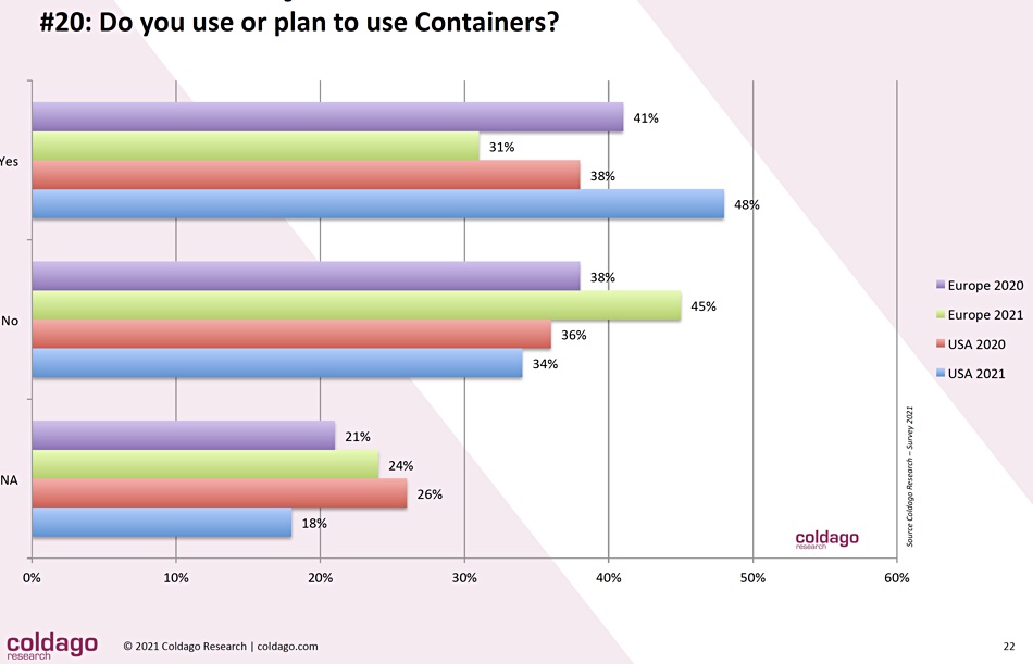
The survey looked more closely at plans for container usage:
Just under half the survey respondents are using or planning to use them, with the European replies declining from 2020 to 2021 and the USA replies growing over the same period. The reason for this European rejection trend is not explained.
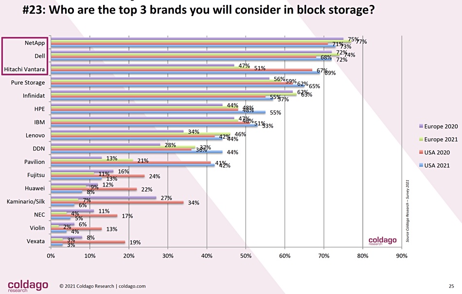
Coldago looked at the supplier rankings in block, file and object storage. In the block area suppliers generally had higher rankings in 2021 than 2020, except for the bottom six: Fujitsu, Huawei, Silk, NEC, Violin and Vexata (StorCentric). This suggests the respondents prefer larger, more established suppliers. Infinidat is now in that list, positioned at number 5, after Pure Storage and above HPE and IBM:
Silk, with the largest 2020 to 2021 change, has recently taken on fresh funding and will be strengthening its sales and marketing efforts. Hopefully it will reverse the trend seen in Coldago’s chart.
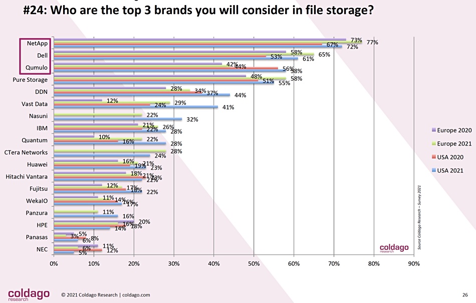
The file storage suppliers were next:
Qumulo has come on strong and is ranked number 3 behind NetApp and Dell. Then comes Pure, DDN, VAST Data and Nasuni, followed by IBM and Quantum. HPE, with no in-house file storage product, languishes down in 16th place, above Panasas and NEC. DDN and VAST Data are both highly ranked.
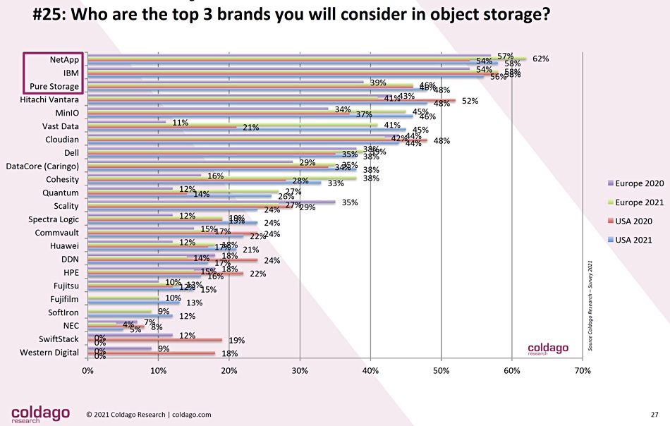
In the object storage sector we see:
NetApp, to this writer’s surprise, leads IBM and Pure Storage. As expected MinIO is high-ranked, being in fourth place. Then come VAST Data and Cloudian, followed by Dell. Cohesity is in the list at position 10, above Quantum and Scality.
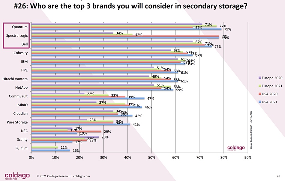
The final chart we look at considers secondary storage suppliers and that has quite a few surprises in its rankings:
First of all Quantum — recovering Quantum — is top, followed by Spectra Logic, and then the first mainstream incumbent supplier, Dell. Cohesity is next, with IBM in 5th place and HPE in sixth position. NetApp is down in eighth place, with the next supplier being Commvault and then MinIO.
This is the one area in Coldago’s survey where the usual suspects, aka established and proven leaders, do not dominate. And we learn that Quantum and Spectra Logic are both very well placed to win business — more so than Dell. Who would have thought that at all likely?
Seagate crossed the $3 billion quarterly revenue line for the first time in six years as demand for high-capacity disk drives spins ever higher. Shipping more bits brings in more bucks.
It earned $3.01 billion in its final FY2021 quarter, ended July 2, and up 19.2 per cent year on year, with a $482 million profit, up 190.4 per cent from the year ago $166 million. Profits were 16.1 per cent of revenues — the highest percentage in three years. The full year revenue number was $10.68 billion — a increase of just 1.6 per cent over FY2020, but with profits of $1.3 billion, up 30.9 per cent year on year.
Chief exec Dave Mosley said: “Seagate delivered very strong June quarter results achieving the highest revenue in the last six years and the highest non-GAAP EPS in nine years, which capped a fiscal 2021 in which we outperformed our expectations.”
Quarterly financial summary:
Gross Margin — 29.4 per cent vs 26.5 per cent a year ago;
Cash flow from operations — $478 million;
Free cash flow — $354 million;
Diluted earnings per share — $2.07 vs $0.64 a year ago;
Cash dividends — $649 million;
Share repurchases — 2.6 million ordinary shares for $228 million.
Seagate told investors this was its third consecutive quarter of record disk drive exabyte shipments, at 152EB, up 20 per cent year on year. The average capacity per drive was 5.4TB. More than 80 per cent of Seagate’s disks were high-capacity drives, generating almost 70 per cent of revenue. These drives were sold into the on-premises nearline market and into public cloud data centres. There was continued demand for mission-critical (fast 2.5-inch) and consumer (external) drives which offset a continued decline in desktop PC drives.
Total disk drive revenues were $2.74 billion, up 18 per cent year on year. Revenue from systems, SSDs and other items was $276 million, a rise of an impressive 42 per cent.
It is shipping dual-actuator 14TB drives, ramping up (single actuator) 18TB HDD production and should be shipping 20TB (PMR, not HAMR) drives in the second half of the year as well. Eventually Seagate expects to ship three types of 20TB drive: conventional PMR, shingled media, and HAMR, into different market sectors.
Earnings call
Mosley opened the earnings call by saying “We are reporting these exceptional results at a time of optimism in parts of the world as vaccinations roll out and economies begin to reopen … While the pandemic remains a difficult reality for many parts of the world and we remain vigilant and continue to manage the business through this period, it is clear the macro level that recovery is underway in the markets that we serve.”
He said Chia demand positively affected drive shipments, but not massively. “new Chia demand represented at most a mid-single digit percentage of total industry exabyte shipments during the quarter, primarily into the distribution channel.”
Mosley also talked about dual-actuator technology. “Remember, fundamentally we believe that by the time you get to 30 or 40 terabytes, you can’t have all that behind one actuator. You need to have dual-actuator at least, and we have to solve all the power problems and all the interface problems with our customers and things like that, to make that happen.“ The 14TB dual-actuator drives go into a specific, but unnamed, market and Seagate is learning about the technology for future use with much higher capacity drives.
Dual-actuator “at least”. Is this a hint that we may see triple actuator drives?
Next quarter’s outlook is $3.1 billion, give or take $150 million — a rise of 34.2 per cent year on year at the mid-point. Moseley said Seagate expects “to grow revenue in the high single-digit percentage range or more in fiscal 2022.”