


A new memory hierarchy is emerging, as two recent developments show. In no particular order, Micron walked away from 3D XPoint and SK hynix revealed new categories and of memory product in a hierarchy of access speed. In both cases the Compute Exchange Link (CXL) is envisioned as the glue that links shared memory and processing devices such as CPUs, GPUs, and app-specific accelerators.
Moore’s Law end game
As Moore’s Law speed improvements come to an end, new techniques are being developed to sidestep bottlenecks arising from the traditional Von Neumann computer architecture. ‘Von Neumann’ describes a system with a general purpose CPU, memory, external storage and IO mechanisms. Data processing demands are increasing constantly but simply putting more transistors in a chip is no longer enough to drive CPU, memory, and storage speed and capacity improvements.
A post-Von Neumann CXL-linked future is being invented before our eyes and it is going to be more complicated than today’s servers as system designers strive to get around the Moore’s Law end game limitations.
Computer architects are devising ways to defeat CPU-memory and memory-storage bottlenecks. Innovations include storage-class memory, developing app-specific processors and new processor-memory-storage interconnects such as CXL, for faster IO. This should enable more powerful, more power-efficient processing systems to run a deluge of AI and machine learning-related applications.
CXL is a big deal, as the in-memory compute supplier MemVerge told us recently: “The new interconnect will be be deployed within the next two years at the heart of a new Big Memory fabric consisting of different processors (CPUs, GPUs, DPUs) sharing heterogenous memory (DRAM, PMEM, and emerging memory).”
MemVerge’s Big Memory technology uses in-memory computing, with memory capacity boosted by Optane storage-class memory to reduce storage IO and so speed applications such as gene sequencing.
Memory developments
The commodity server has a relatively simple design, with CPUs accessing DRAM via socket connections with storage devices sending and receiving data from the CPU-DRAM complex via the PCIe bus. A few years ago, 3D XPoint-based storage-class memory (SCM) arrived on the scene to address DRAM capacity limitations and speed storage-memory IO.
Intel has implemented the technology as Optane SSDS which use the PCIe bus and also as Optane Persistent Memory (PMem), which come in DIMMs and connect to the CPU via sockets. Optane PMem is addressed as memory, with software coping with its slower access latency of about 300ns compared to faster DRAM with a 14ns or so access latency.
In explaining its decision to stop 3D Xpoint development and manufacture, Micron argued that there will be insufficient demand for 3D XPoint chips in the future because memory capacity and speed limitations will addressed by two technologies: High Bandwidth Memory (HBM) and CXL fabrics.
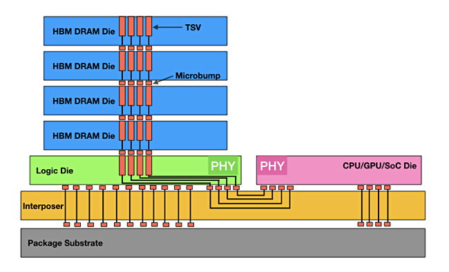
HBM has a faster connection to CPUs than the existing socket-based scheme. This is based on a single SoC design with stacked memory dies sitting on top of an interposer layer that extends sideways to link to a processor. The arrangement provides a lower latency and greater bandwidth connection than the DRAM socket-based scheme. Nvidia GPU servers are using HBM to help them process data faster. Micron’ and SK Hynix both think HBM is slso coming to X86 servers.
Micron and SK hynix see a basic three-layer memory hierarchy running from HBM though DRAM to SCM. SK hynix thinks HBM can also improve energy efficiency by about 40 per cent in terms of power consumption.
CXL enables memory pooling
The Compute Express Link (CXL) is being developed to supersede the PCIe bus and is envisaged by its developers as making pools of memory (DRAM + SCM) sharable between CPUs and also GPUs; but not HBM.
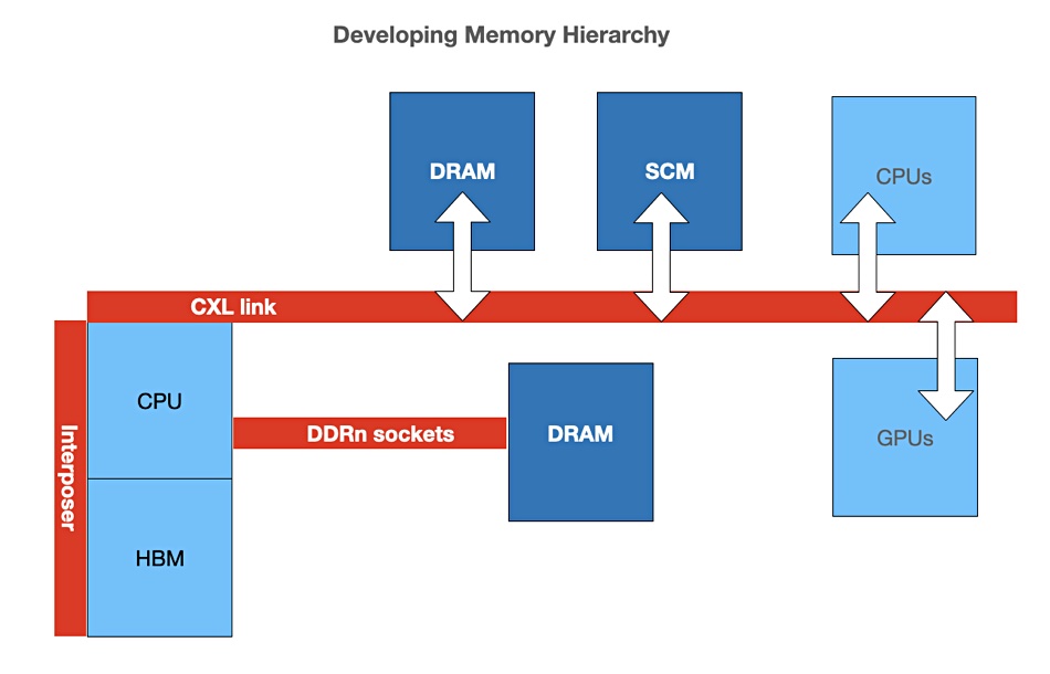
This would mean that individual servers can augment their own local socket-connected DRAM with pools of memory accessed across the CXL bus. These pools could contain DRAM and SCM – but likely not HBM.
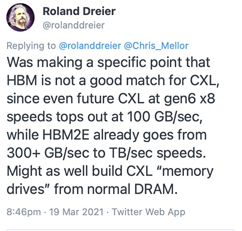
Roland Dreier, a senior staff engineer at Google, has tweeted that “HBM is not a good match for CXL, since even future CXL at gen6 x8 speeds tops out at 100 GB/sec, while HBM2E already goes from 300+ GB/sec to TB/sec speeds.” He suggests the industry could “build CXL “memory drives” from normal DRAM.”
Dreier says: “You could imagine a future memory hierarchy where CPUs have HBM in-package and another tier of CXL-attached RAM, and DDR buses go away. (Intel is already talking about Sapphire Rapids SKUs with HBM, although obviously they still have DDR5 channels.)”
He also sees scope for 3D XPoint with CXL: “a 3DXP drive with a 50 GB/sec low-latency byte-addressable CXL.mem interface seems like a killer product that gives new capabilities without forcing awkward compromises.”
HBM brings compute and memory closer together and so reduces data transmission time between them. But SK hynix foresees even closer links that will reduce data transmission delays even further.
Bring processing and memory closer still
SK hynix CEO Seok-Hee Lee discussed four more kinds of memory, in a presentation this week at the Institute of Electrical and Electronics Engineers (IEEE) International Reliability Physics Symposium (IRPS). The first was Ultra-low Power Memory (ULM) that much less power than DRAM and HBM. The second was a set of memories which are closer to the CPU and, faster to access, than HBM:
- PNM – Processing Near Memory with CPU and memory in a single module,
- PIM – Processing In Memory with CPU and memory in a single package; faster than PNM,
- COM – faster still Computing In Memory with CPU and memory integrated in a single die.
Lee implied that PNM would come first, then PIM which would be followed by COM. Ultimately Lee sees memory technology evolving towards neuromorphic semiconductors which imitate the structure of a human cranial nerve, and possibly DNA semiconductors.
An implementation of PIM is under development by AI chip startup Untether AI, whose TsunAImi PCIe card uses runA1200 chips with processing events distributed throughout SRAM memory.


