


Samsung has produced the largest capacity DDR5 DRAM stick in the world at 512GB.
Update: 26 March; Samsung speed claim queried.
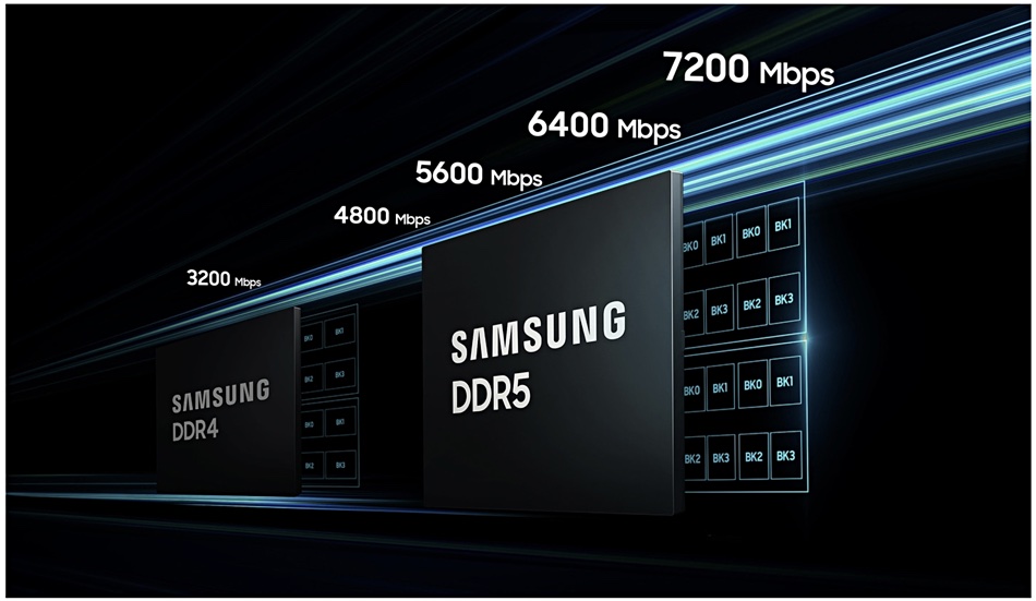
DDR5 or Double Data Rate 5 is faster than the prior DDR4 standard DRAM. A Samsung 128GB DDR4 die in 2015 delivered up to 3,200 megabits per second (Mbps). Samsung claims the new DDR5 module outputs 7,200Mbps, more than twice the DDR4 module’s speed – but there is a problem with this claim as we note below.
Samsung Electronic’s Young-Soo Sohn, VP of the DRAM Memory Planning/Enabling Group, said in a statement: “By bringing this type of process innovation to DRAM manufacturing, we are able to offer our customers high-performance, yet energy-efficient memory solutions to power the computers needed for medical research, financial markets, autonomous driving, smart cities and beyond.
JEDEC, the semiconductor industry standards authority, specified DDR5 to have double the bandwidth and capacity of DDR4. It’s called double data rate because it transfers two messages per clock tick (MT/sec).
Speed claim problem
The JEDEC DDR5 standard specifies speeds between 3,200 and 6,400Mbps and Samsung’s 7,200Mbps is beyond this range. Our Reg‘ sister publication reckons Samsung may have transposed megatransfers per sec (MT/s) and Mbps as 7,200MT/s would be more than double DDR4’s 3,200MT/s.
A January 2020 Samsung document said its DDR5 maximum data transfer speed was up to 4,800Mbps. However, an image and text in an online Samsung document clearly indicates 7,200Mbps;
How can Samsung have exceeded JEDEC DDR5 speed? It appears to have very clever technology or possibly made a transposition error. We asked Samsung if a Mbps to MT/s transposition took place and it denied that had happened.
A Samsung spokesperson said: “We announced that our DDR5 can support up to 7,200 Mbps, which as you can see is significantly more than the initial standard set by JEDEC.”
Module details
Samsung’s DDR5 module is made from 32 x 16GB chips built on a 10nm process. These are made with 8 x 16Gbit DRAM chip dies a few microns thick, stacked one above the other and interconnected with thousands of Through Silicon Vias (TSVs). These are electrodes that penetrate the dies through microscopic holes. TSV technology is an alternative to bonding the component dies together using wires plus a data buffer chip. TSVs enable higher die stacks plus a smaller die footprint and the data buffer functions are included in a master control chip inside the DDR5 chip package.
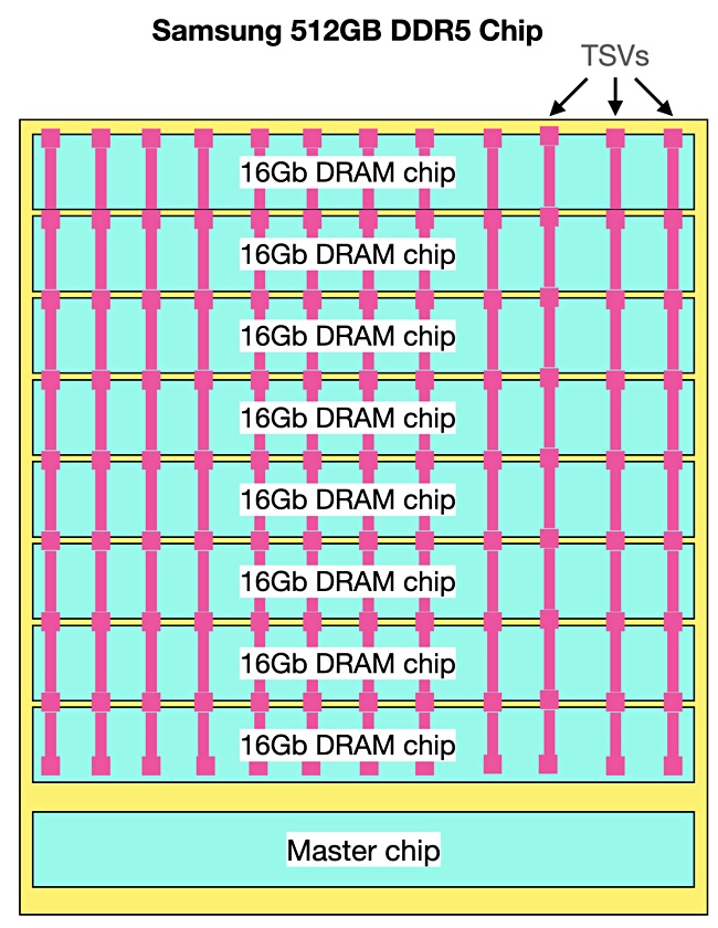
Samsung used TSV die interconnects in DDR4 memory back in 2015. That had 128GB capacity using 8Gb dies.
A High-K Metal Gate (HKMG) material insulates the DDR5 dies from each other, with “K” being a scientific constant indicating insulating capability. As DRAM dies become physically smaller the insulation layer becomes thinner. The HKMG material provides better insulating effectiveness than existing silicon dioxide gate materials, preventing electricity current leakage from the dies. Samsung claims its HKMG DDR5 module will use approximately 13 per cent less power than other DRAM modules, helping data centre power use.
Carolyn Duran, VP and GM of Memory and IO Technology at Intel, said in a press statement that “Intel’s engineering teams closely partner with memory leaders like Samsung to deliver fast, power-efficient DDR5 memory that is performance-optimised and compatible with our upcoming Intel Xeon Scalable processors, code-named Sapphire Rapids.”
Micron started sampling its DDR5 sticks in January 2020. SK hynix announced its DDR5 DRAM in October 2020.
Samsung is sampling different variations of its DDR5 memory product family to customers for verification and, hopefully, certification.


