Home Blog Page 202

Druva offers $10 million SaaS data protection service warranty

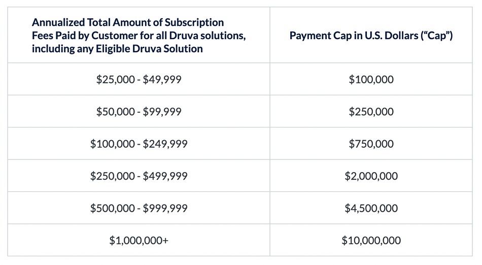
Druva is offering a legally binding warranty that its SaaS data protection service – the Druva Resiliency Cloud – will meet confidentiality, immutability, reliability, durability and availability service levels with up to $10 million in coverage.

Druva’s Data Resiliency Cloud is a cloud-native SaaS offering based on Amazon Web Services public cloud infrastructure. The Data Resiliency Guarantee (DRG) is an expansion of the company’s existing limitations of liability. It enables qualifying customers to protect against a wide variety of data loss and downtime events across five categories of risk, made possible by what Druva claims are best-in-class SLAs. Competitor Rubrik offers a guarantee against its backup data being compromised by ransomware with up to $5 million being payable if data is lost from its backups.

Jaspreet Singh

Jaspreet Singh, Druva’s founder and CEO, said “Ransomware protection alone isn’t enough to satisfy the pressures, challenges and speed of modern businesses.”

In his view, “Protecting data from outside attackers should be table stakes at this point but most vendors are simply unable to make stronger commitments given the limitations of their business models. In contrast, our SaaS model offers complete control over the various technology functions and the ability for our team to manage the entire customer experience.”

The DRG SLAs are:

  • 100 percent Confidentiality SLA to guarantee customer data stored in backups will not be compromised (i.e. malicious and unauthorized access) as a result of a security incident;
  • 100 percent Immutability SLA to guarantee backups will not be deleted, encrypted, or otherwise changed as a result of a cyber attack;
  • 99 percent Reliability SLA guaranteeing successful backup services;
  • 99.999 percent Durability SLA to ensure successful backups will be recoverable;
  • Up to 99.5 percent Availability SLA to maximize uptime.

Singh explained in a briefing that “all of the SaaS vendors, including Druva, have a legal requirement called limitation of liability, that we we are liable if data is lost. … We saw the industry asking for more, like, can you guarantee us reliability of software that the backup success percentage would be 99 percent? Can you guarantee availability of my data? Can you guarantee it won’t be tampered with? Can you guarantee it will not be leaked by employees? So we extended what we typically have called limitation of liability into a full-fledged warranty.”

And that meant that Druva had to be certain its infrastructure and operating procedures were good enough to support offering such a warranty, because it had management ownership of customers’ data. The Druva SaaS system infrastructure had to be available and accessible. The backup service had to be reliable enough, and immutability rock solid, and so forth.

Singh said “We made reliability the number one goal. And we are proud to say we have 99 percent success rate or higher of backup and recovery jobs being successful. And we have zero breach in durability. We have zero lost confidentiality. We have never, ever had a third party get access to data nor have we lost data. So now we are actually firming up our promises by offering a warranty.”

Druva Resiliency Guarantee payout tiering scheme

He explained that Druva had to add extra telemetry to its service to make this warranty possible. “We had to get an understanding of operations to show to customers … we have enough trust and visibility into operations into customer accounts and setups so we can actually back our offering.” It also had to improve its environmental reporting. 

Singh said “There was a fair amount of work involved both in our architecture, operations and visibility into customers to make it a reality.”

We asked Singh if any other on-premises data protection supplier provide such a warranty?

“They don’t, and they cannot, because … you have to be SaaS. … They cannot take responsibility for their confidentiality unless they’re in managed operations. Because we manage operations, we have the visibility and control of all these outcomes. An on-premises data protection vendor couldn’t do the same thing.”

Druva is publishing a master service contract with legal language around the warranty, covering things like scheduled remediation. Singh said this warranty is a sign that the data protection industry is maturing and it means customers can trust Druva more.

For more information on program terms, conditions and eligibility, visit the Druva Data Resiliency Guarantee FAQ web page.

SK hynix’s 238-layer flash gets nominal 6 layer advantage over Micron and YMTC

SK hynix is sampling its 238-layer NAND, shipping 512Gbit chips organised in TLC (3bits/cell) mode to potential customers.

This is 35 percent more layers than its existing 176-layer product. The 238-layer technology was first publicly revealed in April this year, and it has a smaller chip area than the 176L model.

Jungdal Choi, head of NAND Development at SK hynix, said in a keynote presentation at the Flash Memory Summit today that: “SK hynix secured global top-tier competitiveness in [the] perspectives of cost, performance and quality by introducing the 238-layer product based on its 4D NAND technologies.”

SK hynix 238-layer TLC NAND chip

The 4D term refers to SK hynix placing the NAND chip’s peripheral logic circuits underneath the storage cells – peri under cell (PUC). Western Digital and Kioxia have a similar design, called Circuit Under Array, while YMTC puts its peripheral circuitry on top of the NAND stack, building it in a separate CMOS process and then bonding it to the NAND. This design is called Xtacking.

SK hynix’s 238-layer technology produces 512Gbit capacity chips with a bandwidth of 2.4Gbit/s, 50 percent more than the 176- layer product. The amount of electricity used in read accesses to the chip has decreased by 21 percent compared to the 176-layer chips.

The 238-layer die uses charge trap technology as does Kioxia and Western Digital, Micron and Samsung. Solidigm relies on on older floating gate technology. The Charge trap technology is based on storing electrons in a silicon nitride film. Floating gate technology houses the electrons in doped polycrystalline silicon and needs more process steps in its manufacture.

Mass production of SK Hynix’s 238-layer dies should begin in the first half of 2023. Initially the 238 -layer chips will be used in client SSDs for PCs, and then be made available for smartphones and high-capacity server SSDs. SK hynix will produce 1 terabit 238-layer chips next year, which will help with the high-capacity server SSDs.

SK hynix’ Solidigm subsidiary has, we think, 196 layer technology in development. Samsung’s gen 8 V-NAND has 236 layers. Kioxia and Western Digital are at the 212-layer point. YMTC is working on 232-layer technology as is Micron, and this gives SK hynix its nominal 6-layer advantage, not that it really matters in itself as its competitors will be producing 512Gbit chips as well. 

Export issues

A side headache for SK hynix is that it has a DRAM fab in Wuxi, China, and the US government is tightening technology export restrictions to China. This was in an add-on to last week’s Chips and Science Act authorising grants worth up to $52 billion to encourage semiconductor chip manufacturing in the US. Companies accepting money from this fund must not to support semiconductor manufacturing at China below the 28nm level for 10 years. That effectively means the SK hynix Wuxi plant cannot be upgraded with more advanced DRAM manufacturing technology. There is no direct effect on the company’s NAND fabs but, if it moves DRAM manufacturing out of China, as it builds up its US presence, the costs involved could limit its NAND activities.

Cohesity founder and CEO Mohit Aron steps down – Sanjay Poonen takes over

Cohesity founder and CEO Mohit Aron has stepped aside to become the company’s CTO and chief product officer with ex-VMware COO Sanjay Poonen hired as the new CEO.

Sanjay Poonen

Poonen was president at SAP from 2006 to 2013, where he led SAP’s Applications and Platform Solutions & Sales teams, which contributed to SAP’s growth from $10 billion to $20 billion in revenues. He joined VMware as COO in August 2013 and his LinkedIn profile says he led VMware’s growth from $7 billion to $12 billion revenue – meeting and beating expectations in 18 quarters. Poonen left his VMware COO post in August last year, after colleague Rangarajan Raghuram was appointed CEO following Pat Gelsinger’s departure to Intel. He then took a year off, but has decided to get back in the enterprise exec saddle again.

Aron said in his statement: “As we scale, it is important to me to have a tighter focus on where I spend my time to have the greatest impact. I approached the board with the goal of finding a seasoned and proven executive that I could partner with to achieve our ambitious goals. I’m excited to work with Sanjay as we continue to grow and disrupt the $25 billion data management market.”

Two bloggers

Mohit Aron

In a blog Aron explained that his CEO and founder roles meant he had to operate with two mindsets, which created issues. “While I have strived to wear both the breadth and depth hats equitably, there is an inevitable tension in trying to balance them, particularly as the business scales. So, after consideration, I have decided to shift my focus to depth, with the board’s blessing.”

He added this: “I will continue to devote my time to ensuring that we have the greatest products and solutions in the industry as we disrupt the $25 billion market for data management with our next-gen approach. I’m very proud of what we have already achieved, and I know we’re only scratching the surface of what’s possible. More than ever, the world needs to safeguard and make the best use of its most valuable digital asset – data – and I remain dedicated to ensuring Cohesity is a pivotal enabler of that goal.”

We’ll come back to that in a moment.

A statement from Poonen said: “Cohesity sits at the intersection of three of the highest priority business issues today – cyber security, cloud, and data management – and is poised to become a major powerhouse with industry analyst firms naming the company a leader and one of the fastest growing in its category. … I look forward to leading this talented organization and driving even further success in strong partnership with Mohit and all Cohesians.”

Poonen wrote in his own blog that Cohesity “is a company whose value proposition, I can easily explain to my mom and kids: ‘We help companies and governments, protect their data, back it up, archive, search/analyze historical data, and of course, secure it from ransomware attacks.’ I’m super excited about the journey ahead.”

Cohesity has more than 3,000 customers. Four of the top 10 Fortune 500 companies, five of the top 10 US banks, and two of the top 5 global pharma organizations – as well as hundreds of federal/local organizations – are Cohesity customers.

His blog contains what we see as a key passage: “I’ve often told my GTM teams over the years, the world is made up of 5,000 large companies and five million small companies (the surface area of opportunity we were trained to attack at SAP and VMware, where our products became ubiquitous). As such, I see no reason why every company, government and organization – small and big – shouldn’t trust Cohesity with protecting their data! Everyone has data that needs to be backed up, protected from ransomware, archived, and analyzed for risk and insights. Legacy architectures were not optimized for an environment where data is today: in any cloud, any app, any device.”

This ties in with Aron’s view: “Consider the situation before VMware made virtualization commercially available: system resources were inefficiently used, they had limited scale, were difficult to manage, weren’t open to integration, and were very expensive. This is almost exactly the description we use to describe the legacy world of data management. Like VMware, we are bringing a radically new approach to an industry that has seen very little innovation – offering new value in security, simplicity, scale, efficiency, and much more. And with the right leadership and the right technology, I believe we have the right foundation in place to follow VMware’s trajectory.”

Comment

When VMware was founded, hypervisors were nascent and VMware grew and dominated a vastly growing market. Data management, aka data protection, is not nascent. It is mature, with large and well-established competitors. This, in our view, is not like VMware’s starting situation at all.

Think of Rubrik – a startup of similar vintage, size, scope and funding to Cohesity. In the data protection and management area we have Catalogic, Dell EMC, Druva, HYCU, Veeam, Veritas and many more, such as OwnBackup specializing in SaaS app protection.

This is not a world of dumb and stupid and complacent data protection companies. It is both a mature and a vibrant collection of quite fast-developing technology suppliers, all viewing ransomware protection and a multi-cloud approach as table stakes. And all with sticky software that slows down competitive supplier conversions and takeouts.

Poonen and Aron talk about “data”. It’s the new oil. But VMware applies to primary data and Cohesity (mostly) to secondary data. How can Cohesity become  a general data management platform for both primary and secondary data? And should it aim to cover both? If not, then its data management scope gets limited and perhaps needs clarifying.

Also, in the secondary data field, much data – most of it probably – is not inside Cohesity’s market area, such as data warehouses and lakehouses. Should Cohesity get into this space? If it does not then its data management claims are, again, limited in scope.

Cohesity filed for an IPO in December last year. Aron will not be leading his company through that process. We think Poonen’s appointment implies that IPO filing is no longer current. He, and the board, will have new ideas about that. Aand they will involve, we are sure, building a substantial market lead over its competitors and clarifying its market differentiation.

Solidigm client SSD fresh out of the box for longer

Solidigm has launched an updated and affordable gumstick-format client/gaming SSD with data-aware caching that preserves consistent fresh-out-of-the-box performance.

Update; pricing added at end of article. August 12, 2022.

The P41 Plus is a 512GB, 1TB or 2TB capacity drive in the M.2 2280 format with OEM-only 2230 and 2242 size options. It is a DRAM-less drive, relying on the host’s memory, built from 144-layer 3D NAND in QLC (4bits/cell) format, has an SLC cache, and a PCIe 4 x 4 lane NVMe interface. View it as a re-invented and refreshed Intel 670P product. Freely downloadable Synergy software is needed for the drive to operate at its full potential.

Solidigm P41 Plus

Sanjay Talreja, general manager, Client Products and Solutions Group at Solidigm, provided the announcement statement: “The Solidigm P41 Plus delivers performance that matters to end-users while delivering incredible value. Powered by innovative software, the Solidigm P41 Plus provides an exceptional combination of price and performance, in addition to a software-enhanced user experience, that makes our value proposition unique.” 

Let’s get the performance basic numbers out of the way before looking at the wider picture.

  • Random Read IOPS: 390,000 – 26 percent more than 670P
  • Random Write IOPS: 540,000 – 59 percent improvement over 670P
  • Sequential Read bandwidth: 4.125GB/sec – 15 percent better than 670P
  • Sequential write bandwidth: 3.325GB/sec – 23 percent more than 670P
  • Endurance: 512GB –200TBW, 1TB – 400TBW, 2TB – 800TBW (0.4 DWPD) with five-year warranty

These are not high PCIe 4 drive numbers, which tend to be around 1 million read IOPS, 700K write IOPS and 7GB/sec sequential read and write bandwidth. But this, Solidigm stresses, is a value SSD – remember the  “incredible value” comment above. Its performance is tuned for realistic mixed read/write workloads at low queue depths and it won’t drop off as the drive fills.

Why not?

Hinting caching

The key is the Synergy software running in the host PC, notebook or gaming system. Solidigm’s Deno Dean, product line manager for the Client Group, told us in a briefing that typical SSD controller firmware “has no knowledge or concept of file type. What type of file it is? How big is the file? Is it a one meg file or a ten gig file? Is it an mp3 file? Or is it a media file or a boot file? So it it takes all blocks with the same priority.”

This could result in the SLC cache getting filled up with, for example, an 8GB Blu Ray video download, and all the previous data evicted to QLC, where it takes longer to access. The Synergy software has AI attributes and continuously monitors the I/O stack to see what file types and size of data is being accessed on the drive. It then provides hints to the P41 Plus controller’s firmware about what data should be in the SLC cache to keep performance at an optimum level.

Avi Shetty, Solidigm’s senior director of Client Strategic Planning and Marketing, said “It gives the hints back to the firmware, asking the firmware: ‘Hey, retain this file in SLC. Do not move it to QLC. Or this file in the QLC area is important’. We move it back to SLC as a result.”

He said “All the important commonly used high priority workloads, as well as datasets from an end user, are always in SLC – and the beauty about this is it’s continuous learning. It’s not just a fixed lookup table. … it continuously monitors the user behavior and, as a result, adapts.”

And Solidigm is doing this optimization for mixed read/write performance at a queue depth of 1 or 2. Having inspected and run trace analysis on real-life SSD workloads, it found that this is the normal situation – not 100 percent reads or writes.

The net result is that the drive performs very nicely indeed in real life scenarios and Solidigm has the charts to prove it. Here is a PC Mark 10 full system drive benchmark chart: 

The P41 Plus is significantly faster than the earlier Intel 670P. Notice the additional performance jump when the Synergy software is used (rightmost bar). It’s seen in the next chart as well, which looks at Final Fantasy XIV game load time:

A “rhombus” chart looks at the mixed read/write IOPS performance as the drive fills up:

Without the Synergy-enhanced caching (gray line) we see the typical fresh-out-of-the-box performance hit as the drive becomes a quarter full and it then stays at that now sluggish level as the fill level increases. But when Synergy is used (purple line) the performance stays high until the drive is more than half full and then it tails off, creating a rhombus-like outline on the chart.

Solidigm is working with platform partners to bring the P41 Plus SSD to users. Shetty said “We are working with all our platform vendors in this area – AMD, Intel, Google – and, with all our major OEMs. Expect products, expect systems, notebooks, desktops, all-in-ones, two-in-ones, from our various OEMs in both commercial and consumer scenarios coming out pretty much at the end of Q3.”

Also, “By the end of August, early September, you will see the products available in all worldwide retailers, Newegg for example, and … regional partners. And then worldwide system integrators as well.” Shetty mentioned NZXT and Maingear as example SIs.

We can also expect new features to be added to Synergy over time as Solidigm’s software engineers develop it.

Comment

An extraordinary amount of work has gone into the making of this drive. It is no entry-level product based on a slowed-down mainstream product. Rather it is a carefully designed and optimized product for the value market segment, making it a much better than average cheap SSD. 

We think this Synergy software can be used for other SSDs in Solidigm’s range. The idea of shaping cache data set occupancy to match operating data characteristics and tuning it for specific users’ activities over time seems to us to have general relevance to all users. It’s not just for PC/notebook/gaming system users wanting a dependably consistent and affordable drive. 

Bootnote

The 2230 form factor will only be offered in the 512GB and the 1TB capacities. The Synergy software provides drive health check monitoring facilities as well as caching acceleration.

Solidigm said the P41 Plus will go on sale on August 22 with expected retail pricing as follows. 

  • 512GB : $49.99
  • 1024GB : $89.99
  • 2048GB : $169.99

SK hynix announces CXL 2 memory cards and SDK

SK hynix is sampling a CXL v2-connected memory product taking server memory past a terabyte and thereby catching up with Samsung.

CXL, the Computer eXpress Link, is a developing standard protocol to interconnect server CPUs, and their direct-attached memory, with accelerators and other high-speed peripherals, such as pools of DRAM or other memory types. Such external DRAM can be combined with a server’s local or near DRAM in a single and now larger memory pool.

SK hynix’ Uksong Kang, head of DRAM product planning, said: “I see CXL as a new opportunity to expand memory and create a new market. We aim to mass-produce CXL memory products by 2023. 

The company intends to continue to develop DRAM and advanced packaging technologies and then launch various CXL-based bandwidth/capacity expandable memory products.

SK hynix CXL 2.0 memory device.

SK hynix’ CXL memory device has 96GB capacity, composed of 24Gbit DDR5 DRAMs based on 1anm technology; the company’s latest tech node. It is packaged in the ES.3 EDSFF (Enterprise & Data Center Standard Form Factor) format and supports PCIe 5.0 x 8 Lane connectivity. A CXL controller connects the DRAM to the outside world. 

An SK hynix example shows an X86 CPU can have eight DDR5 channels with 768GB of DRAM ( 8 x 96GB DIMMs) and a total 260 to 320 GB/sec in bandwidth. CXL expansion adds in 4 x 96GB CXL memory cards. They add their bandwidth and capacity to the server, enabling it to reach a total of 1.15TB of memory and 360 to 480 GB/sec bandwidth.

SK hynix’s announcement was accompanied by supportive statements from Dell, Intel, AMD and Montage Technologies. 

Raghu Nambiar, corporate VP of Data Center Ecosystems and Solutions at AMD, said: “AMD is excited about the possibilities of workload performance acceleration with memory expansion using CXL technology. We look forward to collaborating with SK hynix on the development and validation of CXL as the industry shifts to a more dynamic and flexible memory infrastructure.”

SK hynix has also developed a Heterogeneous Memory Software Development Kit (HMSDK) for CXL memory devices that allows different grades of memory to be operated in one system. It has features to improve system performance and monitor the systems while running various workloads. SK hynix plans to distribute it as open source in the fourth quarter of 2022 to software developers.

Samsung announced an open-source Scalable Memory Development Kit (SMDK), which virtualises memory attached to the CXL interconnect, in October last year. It launched a CXL expander device in May 2022, with CXL 2.0 support. SK hynix is now catching up.

SK hynix will exhibit CXL 2.0 memory product product at the  Flash Memory Summit this month, Intel Innovation at the end of September and the Open Compute Project (OCP) Global Summit in October.

Phison and Seagate unveil super high performance stats for their PCIe 4 SSD

A combined Phison-Seagate X1 SSD effort is reporting some impressive numbers that would make it the highest-performing standard 4-lane PCIe 4 we have encountered. 

HDD manufacturer and Nytro SSD supplier Seagate did the drive design and testing with Phison, which also provided the controller and built the SSD.

The unit boasts a processor complex with two performance and power-efficient ARM R5 CPUs and dozens of small CPU co-processors that complete computationally heavy, redundant tasks at high speed with, Phison says, a minimum of power consumption.

Phison CTO Sebastien Jean claimed the X1 is the world’s best-in-class enterprise SSD and said it was “created to bolster the industry’s enterprise-class product offerings for a variety of applications such as AI, Cloud Storage, and 5G edge computing.”

High-performance computing is another target market.

The X1 comes in 1 drive write per day (DWPD) read-intensive and 3DWPD mixed-use formats with the latter having lower capacity due to the necessary over-provisioning. The read-intensive version has 1.92TB, 3.84TB, 7.68TB, and 15.36TB capacity levels with the mixed-use version having 1.6TB, 3.2TB, 6.4TB, and 12.8TB capacities.

It has a U.3 format, backwards-compatible with U.2, and the power consumption rating is 13.5W for random reads, 17.9W for random writes and 6.5W when idle. Phison claims it offers more than a 30 percent increase in data reads than existing market competitors for the same power used.

The X1’s quoted performance stats show the fastest random read IOPS and sequential read bandwidth of any 4-lane PCIe gen 4 SSD we have come across:

  • Random read IOPS: 1,750,000
  • Random write IOPs: 470,000
  • Sequential read bandwidth: 7.4GB/sec
  • Sequential write bandwidth: 7.2GB/sec
  • Latency: 84μs read, 10μs write

This is faster than Kioxia’s CD8 PCIe gen 5 SSD, with twice the speed of PCIe 4’s bus speed. The CD8 is an unusually slow PCIe 5 SSD. Other PCIe gen 5 SSDs from Fadu (Echo) and Samsung (PM1743) are much faster and outperfrom the X1.

Liqid’s PCIe  4 LQD4500 “Honey Badger” drive is faster than the X1, but it has 16 x PCIe 4 lanes, 4 x more than the X1, and is a different class of product.

The X1 drive has power loss protection capacitors (pFail), end-to-end data path protection, SMBus, multistreams, SR-IOV, TCG Opal 2.0 support, along with sanitize and crypto erase features.

Phison, which says it has a more than 20 percent share of the SSD controller market, will customize the X1 for specific customers such as channel partners. Get more information here.

OpenCAPI to be absorbed by CXL

The OpenCAPI near memory CPU interconnect group plans to merge with CXL, paving the way to a single processor interface standard for near and far memory, and high-speed accelerator peripherals.

The not-for-profit Open Coherent Accelerator Processor Interface or OpenCAPI Consortium (OCC) was set up in 2016 by AMD, Google, IBM, Mellanox, and Micron to develop an alternative to the DDR channel to link memory to CPUs. There are several other members, including Xilinx and Samsung. Two other standards groups were set up which overlapped its aims: Gen Z and CXL (Computer eXpress Link). They merged in November last year.

Bob Szabo, OpenCAPI Consortium President, said: “We are pleased to see the industry coming together around one organization driving open innovation and leveraging the value OpenCAPI and Open Memory Interface provide for coherent interconnects and low latency, near memory interfaces. We expect this will yield the best business results for the industry as a whole and for the members of the consortia.”

OCC and CXL are entering an agreement, which if approved by all parties, would transfer the OpenCAPI and OMI specifications and OpenCAPI Consortium assets to the CXL Consortium.

OMI, the Open Memory Interface, is a CPU-to-memory bus that connects standard DDR DRAMs to a host CPU. It’s high-speed serial signalling “provides near-HBM bandwidth at larger capacities than are supported by DDR,” according to a white paper: The Future of Low-Latency Memory, co-authored by Objective Analysis (Jim Handy) and Coughlin Associates (Tom Coughlin) for the OpenCAPI consortium. 

Siamak Tavallaei, CXL Consortium President, said: “Assignment of OCC assets will allow for CXL Consortium to freely utilize what OCC has already developed with OpenCAPI/OMI.”

CXL is now in pole position to oversee the development of a single standard for CPU to high-speed intelligent device linkage both inside and outside server chassis in racks.

The CXL consortium has a v3.0 specification coming, according to Design and Reuse. CXL v3.0 features:

  • Fabric capabilities
    • Multi-headed and Fabric Attached Devices 
    • Enhanced Fabric Management 
    • Composable disaggregated infrastructure 
  • Better scalability and improved resource utilization
    • Enhanced memory pooling 
    • Multi-level switching 
    • New symmetric coherency capabilities 
    • Improved software capabilities 
  • Doubles the bandwidth to 64GTs 
  • Zero added latency over CXL 2.0 
  • Full backward compatibility with CXL 2.0, CXL 1.1, and CXL 1.0 

Notably v3 adds symmetric coherency, which Jim Handy told us last month: “means that a single CPU manages the coherency of the whole system. Any limit on the CPU determines the maximum memory size that can be managed.”

Hopefully symmetric coherency will get round this single CPU coherency management problem and increase the total available memory capacity.

As CXL v3.0 is only just emerging into the light we might expect a future CXL 4.0 to include the OpenCAPI assets.

Comment

This is exceedingly good news, and clears the way for a single standard linking processors and intelligent fast accelerators and peripherals with memory, supported by all the manufacturers. It will encourage the formation of a single ecosystem with a wider market for the component manufacturers and a single overall focus for software developers.

Eight months in, Nutanix top sales honcho hops it

Nutanix chief revenue officer Dominick Delfino has quit, just eight months into the job, to join a different technology company. And Nutanix has revised its guidance upwards for the current quarter.

Andrew Brindred

Update: Chris Kadderas’time at Nutanix corrected; 2 Aug 2022.

Andrew Brindred, who was the temp sales head before Delfino came in from running Pure Storage’s sales organization, now gets the CRO spot as well as an EVP title.

Rajiv Ramaswami, Nutanix president and CEO, had to issue the statement about this: “During his five-year tenure at Nutanix, Andrew has demonstrated deep technology sales acumen, a strategic mindset and strong leadership capabilities. … We thank Dom for his contributions to Nutanix, and we wish him the best in the next phase of his career.”

Treasure the irony here as Brindred, despite these qualities, did not get the CRO post when Delfino waltzed into Nutanix. He became SVP and worldwide sales chief operating officer.

Ramaswami extolled Brindred’s virtues some more: “Andrew has a strong command of go-to-market strategies and how to drive customer satisfaction. Coupled with his expertise in developing innovative business strategies and identifying and cultivating leaders, Andrew’s knowledge and experience will be valuable assets to Nutanix as we enter our next phase of growth.”

Brindred himself said “I could not be more fond of, and appreciative for, my time at Nutanix since joining the company in 2017. Nutanix is an outstanding organization with exceptional people, and I’m honored to become CRO.”

Dominick Delfino.

Delfino came into Nutanix in December 2021 and replaced Chris Kaddaras, who had left in October 2021 to join startup Transmit Security. Kadderas was appointed as CRO after 3 years with Nutanix in February of 2020 and he left in October of 2021.

Delfino was hired from Pure, where he had spent just a year, joining in November 2020 from VMware. Five months after he joined Nutanix, in May this year, sales reps were leaving for, Ramaswami said, potential IPO riches at startups. Now Delfino himself seems to have done something similar. Wells Fargo analyst Aaron Rakers said that Nutanix’s sales rep attrition “contributed to the company issuing a F4Q22 rev. guide ~20 percent below the prior Street estimate.”

Nutanix also updated its outlook for its fiscal fourth quarter and full year fiscal 2022 issued on May 25, 2022. Revenue, ACV billings and non-GAAP gross margin are expected to be at or above the high end of the respective prior ranges and non-GAAP operating expenses are expected to be in line with the prior ranges.

William Blair analyst Jason Ader told subscribers: “We remain guarded in our view on the stock given the high management turnover and salesforce attrition, the potential impact of a weaker macro backdrop, and the company’s ability to compete successfully in a cloud-first world.”

Goodbye FTL – Kioxia reconstructing flash drives with software-enabled flash

Kioxia is redesigning SSDs without a traditional Flash Translation Layer (FTL), a minimal drive microcontroller, and an API for hyperscaler host software to have pretty direct flash hardware control for latency, garbage collection and more.

This is part of the Linux Foundation’s open source Software-Enabled Flash (SEF) project, and is being presented at this week’s Flash Memory Summit Conference & Expo. The aim is to get rid of hard disk drive-era thinking regarding SSD controllers, and provide hyperscaler customers with a way to make their flash media operate more efficiently and consistently. SSDs contain flash dies as before, but the existing FTL-running controller is no more, replaced by a minimal processor running low-level SSD operations and a much-reduced scope FTL.

Eric Ries, SVP, Memory Storage Strategy Division (MSSD) at Kioxia America, said in a statement:  “Software-Enabled Flash technology fundamentally redefines the relationship between the host and solid-state storage, offering our hyperscaler customers real value while enabling new markets and increasing demand for our flash solutions.”

A SEF web page identifies five SEF attributes:

  • Workload isolation in both hardware and software domains;
  • Latency outcome control via advanced, hardware-assisted queueing;
  • Complete host control of flash management, garbage collection, and offload features;
  • Faster and easier flash technology migration;
  • Creation of custom, application-centric and optimized flash protocols and translation layers.

An overview web page tells us that the project is based around purpose-built, media-centric NAND hardware, called a SEF unit, focused on hyperscaler requirements, together with an optimized command set at the PCIe- and NVMe-level for communicating with the host.

We are told: “The SEF hardware unit is architected to combine the most recent flash memory generation with a small onboard SoC controller that resides on a PCB module. As an option, the SEF architecture supports an on-device DRAM controller allowing the module to be populated with DRAM, based upon the needs of each hyperscale user. This combination of components comprise a SEF unit that is designed to deliver flash-based storage across a PCIe connection.”

SEF hardware diagram

“Behind the interface, individual SEF units handle all aspects of block and page programming (such as timing, ECC and endurance) for any type or generation of flash memory being used. SEF units also handle low-level read tasks that include error correction, flash memory cell health and life extension algorithms. 

“The small SEF onboard microcontroller that resides on the PCB module is responsible for managing flash-based media. It abstracts and controls generational differences in flash memory relating to page sizes, endurance control and the way that flash dies are programmed. Through the software API, new generations of flash memory can be deployed quickly, cost-effectively and efficiently, providing developers with full control over data placement, latency, storage management, data recovery, data refreshing and data persistence. 

“The SEF unit also delivers advanced scheduling functionality that provides developers with a flexible mechanism for implementing separate prioritized queues used for read, write, copy and erase operations. This capability, in combination with die time scheduling features, enables weighted fair queuing (WFQ) and command prioritization in hardware that is accessible from the API.”

There is an open source, low-level API and an open source, high-level software development kit (SDK).

User application – SEF interface diagram

Read a trio of downloadable white papers to find out more.

  • 7 Reasons for Software-Enabled Flash Technology
  • Introducing Software-Enabled Flash (SEF) Technology
  • Software-Enabled Flash Technology: Introducing the Software Stack

Or watch one of, or all of, up to eight videos discussing the technology ideas involved. 

SEF intro video

Comment

Judging by the white papers and videos above, a lot of marketing effort has gone into SEF already – it looks like a fairly mature project. Only Kioxia amongst the NAND and SSD manufacturers seems to be involved. If the hyperscalers react positively – and we’d guess they have all been approached already – then the other suppliers will probably get involved alongside Kioxia.

At this stage it doesn’t look as if there is an enterprise (on-premises) market for this, as enterprises would be loath to put the effort into developing the software involved. But if a third party were to develop SEF hardware vendor-agnostic software, then that picture could change. We’re thinking of JBOFD (Just a Bunch of Flash Dies) software equivalent to Kioxia’s array-led JBOF (Just a Bunch of Flash) Kumoscale software, but vendor agnostic at the SEF hardware level.

CAMM

CAMM – Compression Attached Memory Module. Kingston Memory says this is a new memory module form factor designed for thin-profile laptops or all-in-one systems. Initially a Dell proprietary design, in late 2022 the CAMM concept was introduced by Dell to JEDEC, the industry standards body for memory modules, to create a new standard for anyone to use.

Initial designs for the industry-standard CAMM, called CAMM2, were made available in late 2023 for computer and memory module manufacturers to adopt, with additional designs in development slated for release by the second half of 2024. 

Instead of leads on the bottom edge of the conventional memory module that plug into a socket, the CAMM uses a compression connector that mounts to a thin interposer on the motherboard. Screws are then used to secure the CAMM in place. A CAMM can be single sided to reduce z-height to accommodate a very thin profile system, placing the DRAM memory components on one side, with options for the width and length of the CAMM module to support higher memory capacities. The JEDEC CAMM2 designs support different types of memory components (DDR5 and LPDDR5/X) to be used on the same socket, which provide flexibility for manufacturers to choose the right memory type for their systems.

Seagate signs orbital satellite storage drive collaboration

Satellite builder Ball Aerospace has signed a memorandum of understanding with Seagate  to collaborate on data processing and storage technology in space.

Update: It’s SSD-based. See +Comment 2 section below; 1 Aug 2022.

Ball Aerospace builds satellites and instruments involved in Earth science and operational environmental missions, environmental monitoring, weather forecasting, emission tracking and water usage observation. It provides environmental intelligence on weather, the Earth’s climate system, precipitation, drought, air pollution, severe storms, vegetation and biodiversity measurements. Seagate is the disk drive market leader and has a small SSD business on the side.

Mike Gazarik, VP Engineering at Ball Aerospace, said in a statement: “There is a need for on-orbit, high-density storage capabilities to meet new mission requirements – in essence space-ready storage that works and acts like terrestrial storage. Therefore, we decided to collaborate on a proof-of-concept solution because Ball has the heritage and experience in designing and building space systems, while Seagate has extensive data storage expertise.”

Ball Aerospace staff prepping a satellite

This collaboration involves planned lab and on-orbit demonstrations to test the concept, which would include Seagate-built technology to support testing of space memory on a Ball-built payload.

Ed Gage, VP of Seagate Research, said: “We consider space the next frontier for data growth, enabled by high-capacity, low-cost secure storage devices. As a leader in our industry and with over 40 years of expertise, we are uniquely positioned to solve the challenges of space systems that store large amounts of data.”

+Comment

Does this mean what we think it means: hard disk drives in orbiting satellites? They are certainly high-ish capacity, at 20TB for Seagate currently, and lower-cost than equivalent capacity SSDs. Disk drives in orbiting satellites need to be built in sealed enclosures so their air-driven head suspension works, and they also need to withstand launch stresses and the low temperatures in space. A third concern is high levels of radiation in space and their electronics need hardening to withstand that. A fourth might be the drive’s inherent angular momentum from its rotating platters affecting the satellite’s positioning.

We can’t really see Ball collaborating with Seagate over SSDs in space, as Seagate has a miniscule share of the SSD market, and doesn’t build its own chips or controllers. It would make more sense  for Ball to collaborate with a NAND foundry and SSD maker. We’ve asked Seagate to confirm that the collaboration focus is on disk drives.

+Comment 2

Ah, we were wrong. A Seagate spokesperson said: “We’re working on a solid state-based SSD-based storage solution concept with Ball Aerospace for LEO (Low Earth Orbit) storage.  We went with SSD because these LEO satellites are small, lightweight, unshielded, unpressurized, and lacking environmental temperature controls. Low-weight is also paramount in this application.”

A Seagate blog says: “Existing products in the radiation-hardened, specialty storage market are typically expensive, slow, and devoid of the most recent technological advancements…. There are obstacles to hardening a commercial solid-state drive (SSD) for space. Commercial SSDs often use low-density parity codes for error recovery and have complex mapping tables and garbage collection. These lead to controllers with millions of gates, which require modern photolithography (i.e., well below 20 nanometers) for suitable performance and power consumption.”

And: “Putting these controllers in a radiation-hardened application-specific integrated circuit (ASIC) or field-programmable gate array (FPGA) is generally infeasible or very expensive. Most radiation-tolerant FPGAs are in older lithography nodes and are challenged for performance and gates. Radiation-hardened ASICs can cost millions of dollars to develop, and with NAND flash chips changing every year or two, can quickly become obsolete.”

“The flash used within SSDs poses an additional challenge. Flash chips are designed for high-volume consumer and enterprise applications here on Earth. Flash vendors spend billions of dollars in developing factories (“fabs”) specifically for these components. The designs of these chips change frequently as new innovations arise. Designing a flash chip specifically for space could cost tens or hundreds of millions of dollars in development.”

So: “We’ve developed a concept for a new secure aerospace data storage device designed with features that make it more robust for LEO and similar environments. 

“The essence of the solution is to use radiation-tolerant/radiation-hard components only where critical or inexpensive and to use error detection and mitigation techniques for radiation-induced events—especially on expensive, unavoidable soft components to minimize their impact. Care has been made to harden the areas of the design that are most critical for reliability and to use less-expensive commercial components where feasible.” 

Los Alamos Labs, SK hynix develop computational storage SSD

Los Alamos Labs and SK hynix will demo a computational storage SSD at the Flash Memory Summit next week with simulation analysis accelerated by three orders of magnitude with indexing of key value stored data.

Los Alamos Labs researches the safety and security of the US nuclear stockpile and carries out weapons research. The organization relies on high-performance computing (HPC) and simulations rather than actual nuclear explosions. Typically the results are stored and analyzed as file-held data but Labs staff, wanting to use big data analytics tools, are moving to store simulation output data in record- and column-based formats to facilitate this.

Gary Grider, High Performance Computing division leader at Los Alamos, said in a statement: ”Moving our large-scale physics simulations from file-based I/O to record- and columnar-indexed I/O has shown incredible speedups for analysis of simulation output.” 

SK hynix KV-CSD prototype, using a long EDSFF ruler format derive attached by a ribbon cable to a processor

The Laboratory has shown 1,000X speedups on analysis of simulation output by leveraging indexing to achieve data reduction on query via its DeltaFS parallel-file system technology.

Computational storage offloads a host server processor by carrying out low-level, repetitive processing operations on a processor attached to the drive, minimizing data movement to the host server and so accelerating processing a notch. Having parallel processing on the drive speeds it up even more.

A relational database stores data records organized into rows and columns and accessed through by row:column addresses. A key value database, such as Redis and RocksDB, stores records (values) using unique keys for each record. Each record is written as a key value pair and the key is used to retrieve the record.

SK hynix research engineers implemented a key value store on an NVMe SSD instead of the traditional block-based Flash Translation layer, and pushed indexing capabilities to a processor attached to the prototype drive. There they joined with Laboratory security science applications and enabled them to run faster, because this technique can save orders of magnitude of data movement upon retrieval for analysis. 

The indexing capabilities enable ordered range queries and point queries which are common operations in simulation output data analysis. Range queries look for all records on a drive with values between upper and lower limits whereas point queries look for records with a specific value.

Grider said: “Demonstrations like this show it is possible to build an ordered KV-CSD that moves the ordering and indexing of data as close to the storage device as possible, maximizing the wins on retrieval from on-the-fly indexing as data is written to the storage. The ordering capability enables range queries that are particularly useful in computational science applications as well as point queries that key value storage is known for.”

Charles Ahn, head of solution development at SK hynix, said: “As large-scale simulation data and big data analytics grow, solutions are critical for these communities. We are very excited about continuing our research partnership with Los Alamos on this high-performance innovation.”

Los Alamos National Laboratory and SK hynix have a memorandum of understanding toward the design, implementation and evaluation of the KV-CSD.