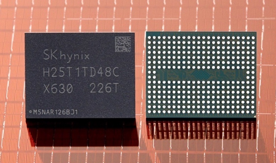
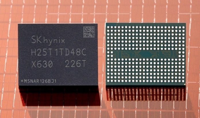
SK hynix is sampling its 238-layer NAND, shipping 512Gbit chips organised in TLC (3bits/cell) mode to potential customers.
This is 35 percent more layers than its existing 176-layer product. The 238-layer technology was first publicly revealed in April this year, and it has a smaller chip area than the 176L model.
Jungdal Choi, head of NAND Development at SK hynix, said in a keynote presentation at the Flash Memory Summit today that: “SK hynix secured global top-tier competitiveness in [the] perspectives of cost, performance and quality by introducing the 238-layer product based on its 4D NAND technologies.”

The 4D term refers to SK hynix placing the NAND chip’s peripheral logic circuits underneath the storage cells – peri under cell (PUC). Western Digital and Kioxia have a similar design, called Circuit Under Array, while YMTC puts its peripheral circuitry on top of the NAND stack, building it in a separate CMOS process and then bonding it to the NAND. This design is called Xtacking.
SK hynix’s 238-layer technology produces 512Gbit capacity chips with a bandwidth of 2.4Gbit/s, 50 percent more than the 176- layer product. The amount of electricity used in read accesses to the chip has decreased by 21 percent compared to the 176-layer chips.
The 238-layer die uses charge trap technology as does Kioxia and Western Digital, Micron and Samsung. Solidigm relies on on older floating gate technology. The Charge trap technology is based on storing electrons in a silicon nitride film. Floating gate technology houses the electrons in doped polycrystalline silicon and needs more process steps in its manufacture.
Mass production of SK Hynix’s 238-layer dies should begin in the first half of 2023. Initially the 238 -layer chips will be used in client SSDs for PCs, and then be made available for smartphones and high-capacity server SSDs. SK hynix will produce 1 terabit 238-layer chips next year, which will help with the high-capacity server SSDs.
SK hynix’ Solidigm subsidiary has, we think, 196 layer technology in development. Samsung’s gen 8 V-NAND has 236 layers. Kioxia and Western Digital are at the 212-layer point. YMTC is working on 232-layer technology as is Micron, and this gives SK hynix its nominal 6-layer advantage, not that it really matters in itself as its competitors will be producing 512Gbit chips as well.
Export issues
A side headache for SK hynix is that it has a DRAM fab in Wuxi, China, and the US government is tightening technology export restrictions to China. This was in an add-on to last week’s Chips and Science Act authorising grants worth up to $52 billion to encourage semiconductor chip manufacturing in the US. Companies accepting money from this fund must not to support semiconductor manufacturing at China below the 28nm level for 10 years. That effectively means the SK hynix Wuxi plant cannot be upgraded with more advanced DRAM manufacturing technology. There is no direct effect on the company’s NAND fabs but, if it moves DRAM manufacturing out of China, as it builds up its US presence, the costs involved could limit its NAND activities.


