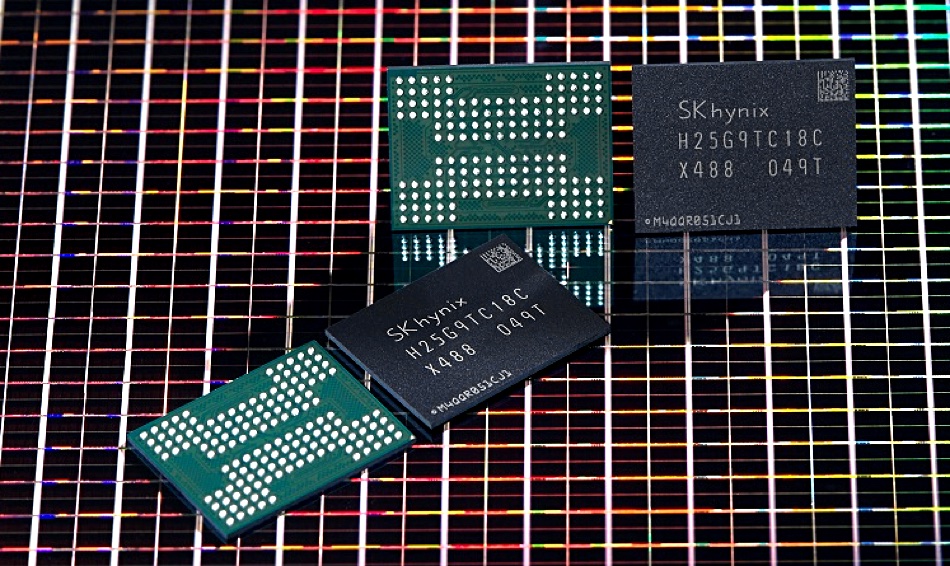
Anything Micron can do SK hynix thinks it can do better. And so the company has announced its own 176-layer 3D NAND technology, sending 512Gbit TLC (3bits/cell) die samples to SSD controller companies in recent weeks.
Micron began volume shipments of 176L NAND last month and so has several months advantage over SK hynix and Samsung. The latter has said it will probably ship 176L NAND in the second quarter next year.
SK hynix said it will ship 176L SSDs for mobile products by the middle of next year, and they will have improved maximum read speed by 70 per cent and maximum write speed by 35 per cent, over the 128L product presumably.
Consumer and enterprise SSDs will follow later in 2021. SK hynix will also develop a 1Tbit die using the176L technology. B&F thinks this might use QLC (4bits/cell) technology to get 33 per cent of the capacity increase, with the remainder coming from more cells in each of the 176 layers.

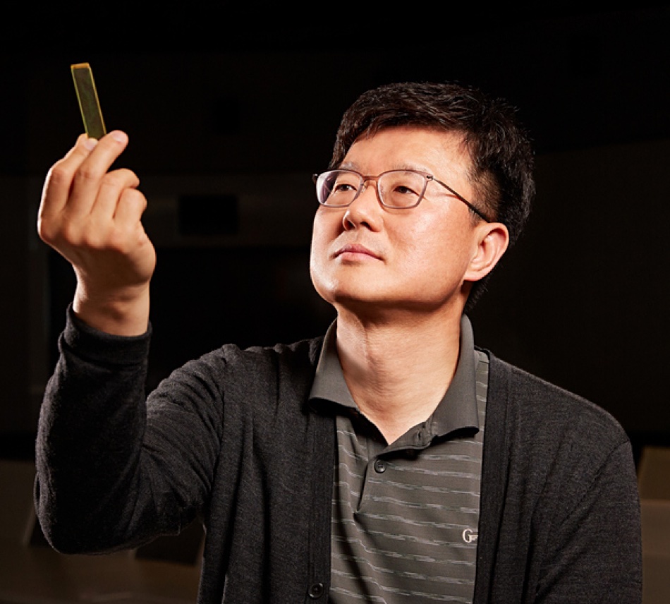
Jung Dal Choi, head of NAND development at SK hynix, put out a statement: “NAND flash industries are striving to improve technologies for high integration and maximum productivity at the same time. SK hynix, as a pioneer of 4D NAND, will lead the NAND flash market with the industry’s highest productivity and technology.”
To justify this claim, SK hynix is bigging up the performance and technology advantages of its 176L product. For example, the company claims:
- The industry’s best number of chips per wafer
- Bit productivity improved by 35 per cent compared to SK hynix’s 128L technology
- Cell read speed increased by 20 per cent over 128L NAND by adopting 2-division cell array selection technology
- Data transfer speed also has been improved by 33 per cent to 1.6Gbit/s
By ‘4D NAND’, SK hynix is referring to the placement of the peripheral CMOS logic for the die underneath the stacks of cells, just like Micron. This helps to decrease the die’s footprint and SK hynix dubs the technology ‘Peripheral circuits Under Cell’ (PUC).

SK hynix’s 176L technology is based on charge trap cells, like Micron, and the cell stack is actually based on two separate 96-layer strings, again like Micron’s 176L product.
The 2-division cell array selection technology involves logically divides a cell into two to make reads faster. The halving means the call has a lower resistance, which shortens the time needed for a sensing voltage to be applied and so improves the read speed time.
The claimed die-level performance and technology advantages are all very well. But how will they translate into speed and cost benefits for SSDs? Let the benchmarks begin!


