Software defined storage is driving a revolution, and dragging traditional hardware along with it.
WEBINAR Storage architectures must constantly evolve to meet rapid changes in enterprise demand for faster, more scalable capacity in line with application and workload requirements. But how do IT departments manage the virtuous cycle that sees software innovation continuously spur advances in storage hardware, which in turn drives further development of storage software in endless rotation?
A distinguished line of industry experts including Anders Graham from Kioxia, Tahmid Rahman from Solidigm, Rick Kutcipal from Broadcom, and Paul McLeod from Supermicro will come together to discuss this issue on 17 August in a session moderated by The Register’s Timothy Prickett Morgan.
They’ll outline how manufacturers are optimizing storage server design using the latest SSD, HDD and SDS technologies, protocols and standards, including QLC and 24G SAS, and discuss the role of PCI-e, NVMe and CXL in next generation disk and storage architectures.
The respective companies will go on to reveal some of the detail behind their commercial and technology partnerships and consider how Supermicro is helping suppliers reach new customers for their storage products and services.
If you’re interested in hearing more, click here to sign up and listen in on August 17.
Eight months after filing for its IPO, data protection and management company Cohesity has hired its first external CEO: Sanjay Poonen, with founding CEO Mohit Aron transitioning to CTO and Product Officer. We had the opportunity to meet these two execs at Cohesity’s San Jose HQ and discuss Poonen’s ambitions for the company.
We’ll structure this interview in two parts, with the first focusing on Mohit Aron, and the second on Sanjay Poonen and his thoughts.
Mohit Aron
Cohesity presents itself as a data management company. Blocks & Files suggested that Cohesity doesn’t manage primary data, data in databases, transaction data, data in data lakes, or data warehouses. It primarily manages data that’s been protected by Cohesity. The bulk of an enterprise’s data does not appear to be covered by Cohesity, so how can it call itself a data management company?
Founding and now ex-CEO Mohit Aron said: “Cohesity is a data management company, and I think data management does not equal backups. We actually do way more than backups. In fact, our mission – the mission of the company – was that there are too many silos in IT infrastructure. One of the silos is backup.”
There are other silos like managing files and objects, test and development, and silos on doing analytics. Cohesity, Aron said, brings all these together. “We do analytics, we can do protection against ransomware. And security. We store production objects, we do handle production data for many of our customers, they store their files and objects on us.”
Aron said: “We have over 700 customers, I believe, that … store their files and objects on us … something around 25 to 30 percent of our customers use us for more than one use case. I think, from a business point of view, yes, we may have started primarily as backup … but we are a data management company.”
The iPhone analogy
He compared Cohesity to a smartphone. “A smartphone started off by being a telephone. But beyond that, it’s also a GPS. It’s also a camera. It’s also a flashlight, it’s also a music player. So … if you buy a smartphone, you’re probably not buying a camera … Some people may find some value in those products still and still may buy them, but by and large [they don’t].”
Some companies may still buy independent filers, object storage systems, and so forth, but many will use the ones that come with Cohesity – in the same way they use smartphone apps, built on and integrated with the smartphone platform.
Therefore, Aron said, “We are a data management platform. And there are some things we do today to address the $25 billion TAM. And as and when we innovate, that can possibly increase to a much bigger TAM, right? So there are possibly things that the world out there does to the data that we may not be doing today. But that doesn’t change the fact that we are still a data management platform. Nobody can do everything. You know, by by your argument, nobody can be called the data management company.”
He pointed out that the smartphone only had a handful of apps when it was introduced. Now it has millions. “So I would say the same thing about us – we have barely scratched the surface of what we can do.”
He said some companies “may call themselves data management because they do one thing. But the point is they don’t have a platform for doing anything more … I think it’s all about being a data management platform, which may start off by doing a few things with data. But over time, it’s been architected to do more things so that you don’t have to keep building silos.”
He is a strong believer in an ecosystem, in company partnerships. And Cohesity has a marketplace, launched in March 2019, from which customers are able to download apps and run those apps integrated with the Cohesity platform. For example, Cohesity partners with Model9 to do mainframe backups, and Model9 is in its marketplace.
Aron says that in order to have an app marketplace, you need to be a software platform on which you can run third-party software via APIs. Cohesity sees most of its data management and protection competitors have built products, architected them, as just a place to store bits and bytes. In contrast, Cohesity architects its software with the assumption that it’s going to be a general purpose platform on which customers can run other software.
Aron said: “It’s not just a dumb place where you put the data. It also is a place where you want to compute. And it’s not just our compute, it’s also compute from third parties.”
We checked. There are 26 apps available in this marketplace, 19 of which have been developed by Cohesity. That means getting on for three-and-a-half years after its launch, Cohesity has seven apps available from third parties and the ecosystem is fairly small.
Cohesity has a land-and-expand strategy. Sell to new customers for new workloads and/or by competitive takeout and, once present, expand the applicability and use of its software platform. Aron said one big financial customer moved from seven different backup products to just using Cohesity. Another a big financial customer had 75 different islands of Data Domain systems that they had to manage independently. Now they use Cohesity instead.
Having set the scene, part two of this interview will turn to Sanjay Poonen and how he intends to grow the company.
Micron and Western Digital (WD) want some of the $280 billion US CHIPS and Science Act funding to go towards semiconductor research for memory-centric computing.
Update. WD replied with a ‘no comment’ type reply to our query about involvement with Micron and the MCOE. See the last but two paragraph. 9 Aug 2022.
The two are pushing for a Memory Coalition of Excellence (MCOE) funded by the National Semiconductor Technology Center (NSTC), which is being set up by the CHIPS and Science legislation funding. The arguments are outlined in a jointly authored report by memory maker Micron and storage vendor WD titled Memory Coalition of Excellence Recommendations for the National Semiconductor Technology Center.
Scott DeBoer, who runs Micron’s Technology and Products organization, writes: “Memory is not only ubiquitous, it is at the leading edge of semiconductor manufacturing, requiring production of advanced technologies that are pushing the laws of physics. … we now have a historic opportunity to regain global semiconductor leadership through the passage of the Chips and Science legislation and subsequent funding of the NSTC.
“The NSTC will be a public private-sector consortium focused on enablement of advanced semiconductor technology. It will play a pivotal role in driving US technological innovation and leadership over the long term. Furthermore, it will support the US in refining and accelerating its global technology and semiconductor leadership.”
Micron and WDwant the NSTC to focus on memory-related semiconductors: “The establishment of a Memory Coalition of Excellence (MCOE), as a pillar within the NSTC, is critical for foundational memory technologies and will further enhance American economic competitiveness and national security. The MCOE will bring together industry leaders, academia and national labs further supporting the US in refining and accelerating its global technology and semiconductor leadership.”
In DeBoer’s view: ”The NSTC should develop and articulate a long-term (>5 years) vision and roadmap for the future of next-generation semiconductor technology.” Some key activities for the MCOE are said to include:
Research and development for materials, process/metrology technologies, and new analysis techniques
Modeling methodologies and tools
Next-generation 3D memory technology development
New memory design concept enablement
Near and/or in memory compute prototyping
Heterogeneous integration at wafer and chip level
Advanced packaging
The report
The 16-page MCOE report is recommended reading for anyone involved in NAND and DRAM development. There are 10 contributors, five from MIcron and five from WD. The WD contribution is all about NAND, not hard disk drives. WD has a joint venture with Japan’s Kioxia to make 3D NAND chips, and uses its half of the foundry’s output to make SSDs. WD has no NAND fabs in the US whereas Micron has two; one in Manassas, Virginia, and the other in Boise, Idaho.
The report says microelectronic chips and semiconductor technology are crucial for the US’s competitiveness: “Semiconductors play a pivotal role in US national economic activity and national security… The United States’ competitiveness in memory faces several challenges compared to other countries, including economies of scale and more limited investment incentives.”
It points out: “The cost of continually redeveloping and improving logic chips over the past decade has become exorbitant, limiting production capabilities to only a few of the world’s largest companies.”
It argues that the US government does not provide enough R&D help: “While the federal government accounts for 13 percent of total semiconductor R&D investment in the US, this percentage is well below the 22 percent average across all other technology sectors.” Therefore: “It is imperative for US federal investments to prioritize memory and storage R&D.”
“The ubiquitous nature of memory in electronic systems means that memory cells make up approximately 85 percent of the entire device count in semiconductor manufacturing. However, US-based manufacturing of memory only accounts for 2 percent of the global total… Federal initiatives, such as the proposed NSTC, provide a unique opportunity to support sustained domestic memory technology innovation, thereby bolstering US national and economic security.”
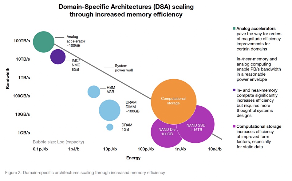
The bulk of the report deals with DRAM and NAND technology matters and declares that there is a memory wall holding back computing development: “Current data handling schemes rely on an architecture in which data storage is separate from data processing. This creates a need to constantly shuttle information to and from memory, which happens at great performance cost, in both time and energy. ‘The memory wall’ refers to this time and energy bottleneck in the system.”
Memory-centric architectures exist to bypass this memory wall:
Computational storage
Near-memory compute
In-memory compute
Analog accelerators
Analog accelerators are part of domain-specific architectures tailoring the architecture to characteristics of the workload. Each of these four items is increasingly efficient in terms of the energy needed per byte (picoJoules/byte or pJ/b):
MCOE report graphic
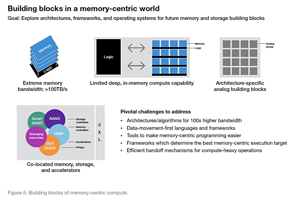
The report says: “Memory and storage chip technologies have transitioned into a post-Moore’s law regime: the 3D scaling paradigm… Continued progress on this path requires a complete reimagination of the interaction between compute, memory, and storage.
“Memory-centric compute is the logical path to perform advanced computing at low energy and high performance for memory-bound workloads, including AI inference and training.
“Any serious move toward memory-centric compute requires integrated innovation from applications to the storage bits, including architectures, frameworks, operating systems, and memory systems. All items in the compute stack must evolve together in a system-level driven memory-centric paradigm.”
“Bringing workloads closer to memory has begun with stacking memory chips in a 3D fashion, termed high-bandwidth memory (HBM), and integrating these stacks with systems in a 2.5D manner… one can imagine the complete merging of memory and logic where analog memory functions are arranged to provide concurrent compute capability.”
MCOE report building blocks diagram
What the report writers want is for the MCOE to “focus on pre-competitive research in materials, process, 3D structures and manufacturing technologies for memory and collaborate with other COE’s (Centers of Excellence) on packaging and interconnect technologies to enable next generation of energy-efficient computing and domain-specific accelerators… The MCOE should also identify a set of nation-wide grand challenges facing memory performance scaling that encourage large-scale collaboration across the US semiconductor ecosystem.”
The MCOE will be an institute with advanced facilities: “The facilities and infrastructure should provide advanced memory/storage, logic, and analog system prototyping with enablement of supporting materials, devices, and packaging. The envisioned infrastructure for such goals includes state-of-the-art, 300 mm clean room space with leading-edge semiconductor tooling capabilities to fabricate full-flow, concept memory chip prototypes, components and modules, as well as a dedicated systems lab for verification and testing”
The report writers think there should be “a fast ramp from lab to fab.”
Report conclusion
1. A concerted drive by the NSTC can accelerate innovation in memory and storage by enabling next-generation memory-centric design architecture, 3D memory structure technology development, and heterogeneous integration.
2. The NSTC should create a Memory Coalition of Excellence to support focused attention on the aforementioned memory-centric innovations needed for compute infrastructure of the future.
3. Investment in memory advancements will prevent semiconductor-based technology from stagnating and secure the continued cadence of technological advancements, thereby ensuring continued US economic and national security.
Western Digital involvement
Why is Western Digital involved? It has no fabs in China and therefore no danger of fab IP leaking. As far as we here at Blocks & Files can see, the only incentive is a closer relationship with Micron.
It is hard to see why the US government should fund domestic R&D to help give the WD-Kioxia JV access to new technology for its Japanese fabs. But if WD were to get closer to Micron, such as sourcing NAND chips or even building a joint fab in the US, that would be a different matter. We have asked Western Digital to comment and a spokesperson replied: “We appreciate your interest. We don’t have any further comment to provide. Everything we have to say on this matter is in the white paper.”
A no comment comment.
One other piece of background context: activist investor Elliott Management is pushing for Western Digital to separate its HDD and NAND/SSD operations into two separate businesses. WD’s board is examining strategic options for the corporation. One of these options may involve a closer alignment with Micron.
Some three thousand people from the flash and SSD supply industry gratefully met at the Flash Memory Summit 2022 in the Santa Clara convention Centre this week – the first FMS summit for two years due to the great COVID convention shutdown.
The vibe was overwhelmingly positive. Attendees were pleased to be there, to be part of the flash community, and there was a strong sense of everyone associating together for the greater good of the flash and SSD ecosystem. Sure, there were pretty direct questions in some of the many sessions, but there was obvious respect on the part of both question asker and question answerer. Everyone, it appeared, was simply glad to be there and taking part.
The summit focus was on suppliers in the flash and SSD ecosystem, not end users. But any end users who did attend enjoyed an unrivalled opportunity to look into the heart of the technology developments.
These were centred on CXL, computational storage, the post-Optane situation, and an astonishing amount of development in the number of types of SSD, the componentry for CXL, and hardware to make flash more effective as a hot data store – and also a cold data store, surprisingly. That came in the shape of a 128TB – yes 128TB – Samsung archive SSD.
We have already reported on some developments: SK hynix’s 238-layer flash; SK hynix announced CXL 2 memory cards and SDK–CXL memory device; Solidigm’s neat FOB-extending P41 Plus client SSD; Phison and Seagate unveiling super high-performance stats for their PCIe 4 SSD; and, in a very well-timed move, OpenCAPI merging with the CXL organization.
There was one single negative event: the ousting of the founders of computational storage startup NGD amidst funding round troubles. Computational storage (CS) has its supporters and its critics. One of the latter told me CS is crumbling around the edges. Another said CS has to be programmable and needs a killer app, which it lacks. Hardware-enabled compression and encryption is not computational storage – it’s relatively trivial hardware acceleration. Good as far as it goes – which is not very far at all.
But CS partisans were many, and pointed to Pliops and ScaleFlux product advances, Solidigm signalling it’s interested, IBM flash module support, and SK hynix support. More suppliers are piling into the CS market than are getting out, but opinion is still divided – unlike CXL.
MemVerge led a CXL charge, with a whole day of presentations and panel sessions. It was accompanied by suppliers announcing CXL memory componentry and general support. The general thrust is that CXL is a great and good technology. It has a large and strengthening supplier ecosystem and wide industry support. I heard not one single negative CXL sentiment during the summit.
Optane’s departure has been met with a sentiment best described as “glad it’s over” – the technology’s demise had become almost certain following the killer blow of Micron withdrawing from 3D XPoint fabrication and selling off its Lehi fab. The prospect of any other supplier spending $5 billion to convert an existing fab – or $10 billion, $15 billion or more to build a greenfield 3D XPoint fab – is ridiculous. It isn’t going to happen.
The gap in the memory storage hierarchy that was plugged by Optane will be filled from below by faster SSDs – Neo’s multiplying SSD plane technology looked highly relevant to this. And it will be filled from above, for customers that can afford the high prices and low density, by MRAM and other resistive RAM technologies. The central area in this gap looks likely to stay unfilled – because there is no affordable and fast enough storage-class memory technology in existence.
Right, says the flash industry. Optane is over and done with. We’ll make do with memory expansion via pooling DRAM on CXL v2 and 3. Move on.
There were standout technology advances. For example: NeuroBlade and its GPU-style processors and hyper-compute for analytics; GRAID and its AI-style processor plus optimizing the whole digital data supply chain between flash and processors; FADU and its controller promising greased lightning PCIe 5 SSDs.
Winbond was there, reminding everybody NOR flash has a role to play in every smart device. Yangtze Memory Technology was there, secretive almost to a fault about its X3-9070 v3 Xtacking product or technology. What is the flash cell layout inside? Is it QLC or TLC? We can’t say. How many layers does it have? We can’t say. There have been reports you are developing 196 ad 232-layer flash? No comment. Will these be co-ordinated with Xtacking v3 and v4? We can’t say.
This reticence contrasted with the general openness seen with the other suppliers, all of whom were keen to present their technology and explain how it worked.
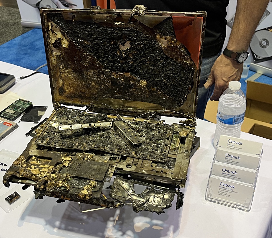
The funniest stand was Ontrack, with its drive recovery technology and a battered, burnt and broken notebook as its prime exhibit:
Ontrack burnt notebook from which data was recovered. (We should point out that the read speed was fairly low – something like 500GB/day, or worse!)
The Flash Memory Summit is a community of suppliers all working for the greater good of the industry. This rising-tide-lifts-all-boats atmosphere was refreshing – it’s not something I’ve seen at other storage shows, such as VMworld or similar supplier events. All FMS 2022 attendees were believers in the flash religion, if I could put it like that, and the industry is in a very positive and solid state.
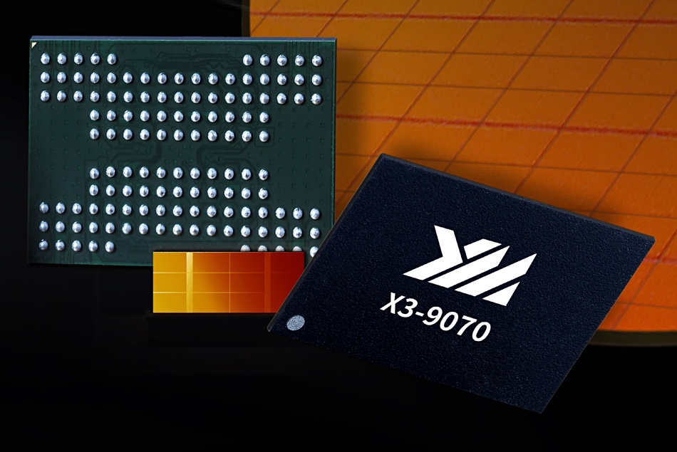
YMTC unveiled its X3-9070 TLC 3D NAND flash at this week’s Flash Memory Summit and would not reveal any substantive details about it – at all.
X3-9070 flash uses YMTC’s Xtacking 3.0 architecture, which is based on sticking the 3D NAND flash underneath a separately fabbed CMOS peripheral circuit logic chip and bonded to it with millions of small connectors, or Vias. Confusingly, Xtacking v3.0 is YMTC’s fourth generation of its 3D NAND.
A statement from Thomas Chen, EVP of YMTC, said: “We are confident that our commitment to accelerating the evolution of Xtacking will help position us as a leading provider of memory solutions and a key value contributor to the global semiconductor industry.”
The X3-9070 has a 1Tbit die – the highest density in YMTC’s history, built from 232-layer 3D NAND according to Reuters based on Chinese state-backed media outlet Global Times. YMTC refused to confirm this.
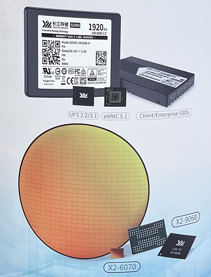
It has a 2,400MT/sec I/O speed – 50 percent more than YMTC’s previous generation of products – while lowering power consumption by up to 25 percent. YMTC is currently shipping and selling 64- and 128-layer products, which presumably used Xtacking v1.0 (64-layer) and Xtacking v2.0 (128-layer) designs.
For example, X2-6070 and X2-9060 products:
So the XC-9070 has a potential for 25 percent lower power consumption than the X2-9060 SSD.
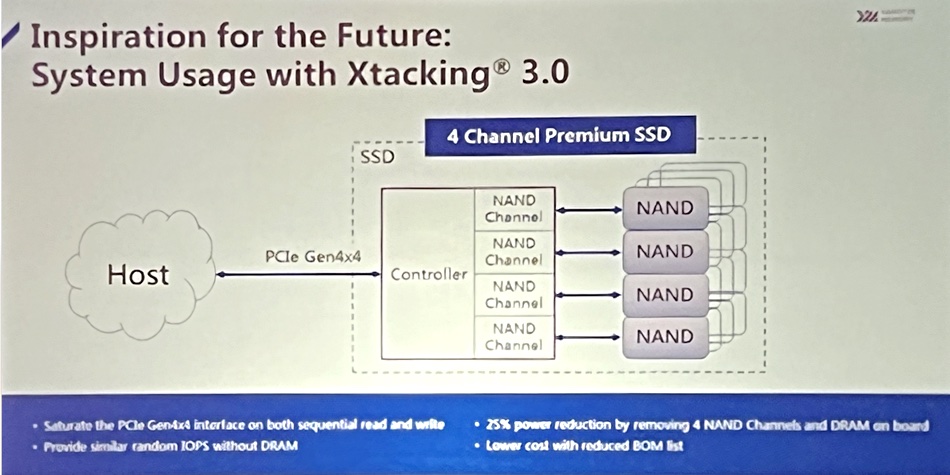
Xtacking 1.0 delivered 800MT/sec with Xtacking 2.0 doubling this to 1,600MT/sec. YMTC explained in a presentation that Xtacking 3.0 transitioned from a prior Front Side Deep Trench process to a Back Side Source Connect (BSSC) design, which involves a simpler production process and is lower cost.
Version 3 reduces the CMOS die size compared to v2, which allows more NAND planes and features to be supported. The X3-9070 die has six independent planes with asynchronous multi-plane independent (AMPI) operation supported on each plane. This improves both random and sequential IO.
A DRAM-less PCIe 4 x 4-lane SSD design was shown as an example of building an SSD product on the Xtacking v3.0 platform;
iPhone picture of a YMTC presentation screen
The controller has four channels, each of which links to NAND dies. And the SSD can saturate the PCIe 4 x 4 interface and also can provide the same level of random IOPS as an equivalent (but non-Xtacking) SSD with on-board DRAM.
We have not been provided with any actual IOPS or bandwidth numbers for the X3-9070, nor any data on endurance, capacity options or enclosure format. This leads us to think that it may not be a deliverable product – more of an outline design base on which to develop shippable SSDs.
YMTC booth staff at FMS 2022 were not able to answer any detailed questions at all or even simple ones, such as the X3-9070’s layer count. Such secrecy inevitably raises doubt about the status of the product.
An add-on to the US CHIPS Act prevents suppliers shipping technology to China enabling its companies to build 128-layer or greater 3D NAND. YMTC has said it’s building a second NAND fab and its fitting out could be affected by this restriction.
Flash market leader Samsung excelled itself at the FMS 2022 event this week, showing a near blizzard of new products: a petabyte-scale SSD, a memory-semantic SSD, a SmartSSD, and SSD telemetry plus general availability of a PCIe 5 SSD and a 24GB SAS SSD and CXL DRAM. It had a fairly crowded booth at the event and we went around, iPhone camera in hand, and snapped everything that looked interesting.
There’s a lot to cover here so get yourself a coffee and set ten minutes aside to read it.
We’ll start with a statement from Jin-Hyeok Choi, EVP of Memory Solution & Product Development at Samsung Electronics. He said: “The IT industry is facing a new set of challenges brought on by the explosive growth in big data, and this underscores the importance of a robust, cross-industry ecosystem. We are committed to developing transformative memory technologies that can bring far-reaching changes in how we move, store, process and manage data for future AI, ML and HPC applications, as we navigate these challenging tides together with industry partners.”
Well, transformative, yes. The drives Samsung exhibited are certainly not your everyday SSDs, as we’ll see.
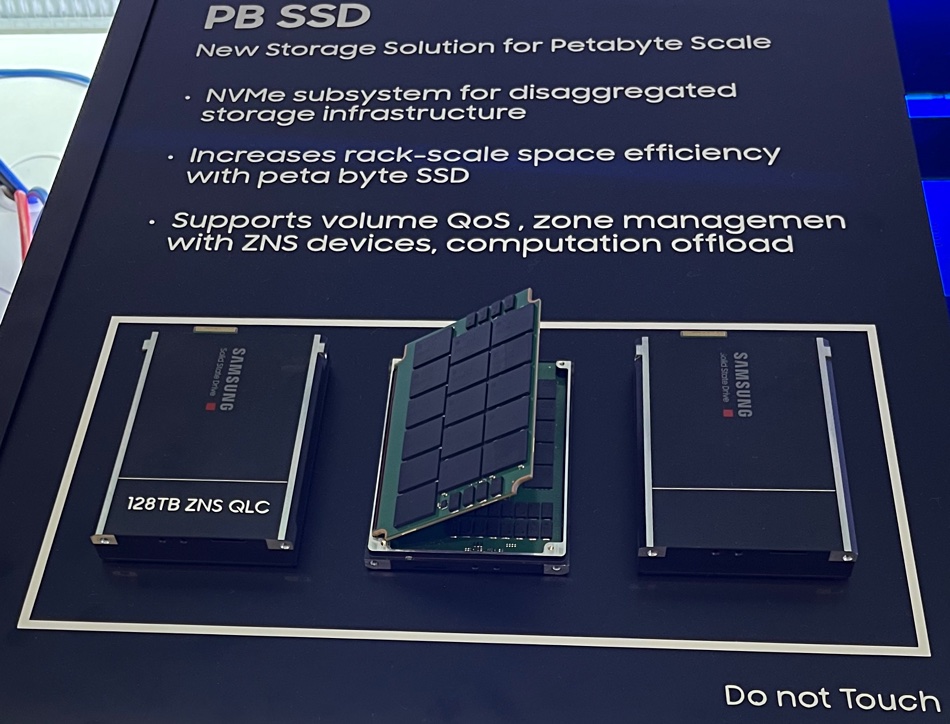
Petabyte-scale SSD
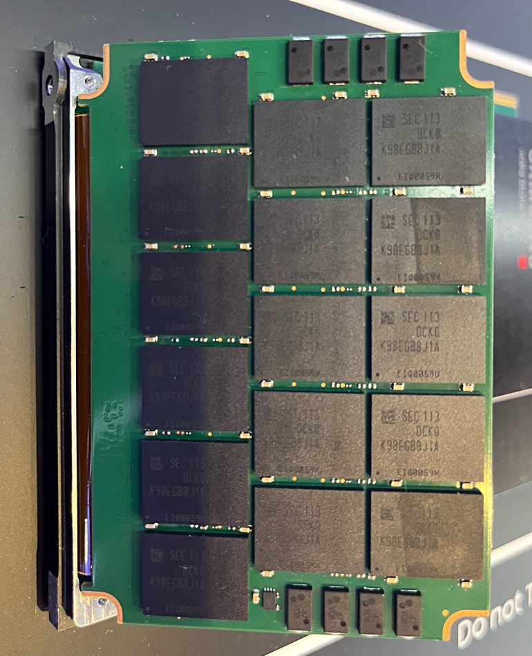
Samsung’s petabyte-scale SSD is is a 128TB drive, using QLC (4 bits/cell) NAND, supporting zoned name spaces and with a PCIe/NVMe interface. It is an EDSFF format package with two circuit boards inside, which are connected with a card-width ribbon cable, giving Samsung’s engineers four card surfaces to play with.
iPhone photo of 128TB SSD display
Samsung presents it as being capable of computational storage. The zoning means it can support different quality of service standards for zones, as set up by a host.
16 NAND chips on the surface of one of the cards in the 128TB drive
The 128TB capacity is four times that of today’s largest SSDs which top out at 30.7 or so terabytes. Nimbus sold a 100TB SSD back in March 2018. Toshiba, in pre-Kioxia-split days, and in the same month suggested it could build an 85TB SSD. We don’t recall this coming to the market.
Samsung’s announcement claimed the drive would “allow a single server unit to pack more than one petabyte of storage, enabling server manufacturers to sharply increase their storage capacity within the same floor space with a minimal number of servers. High server utilization will also help to lower power consumption.” Indeed.
Back-of-the-envelope math says a 2U x 24-slot chassis filled with Samsung’s 128TB drives would give you 3.07PB of capacity. Fill a rack with 20 of these enclosures and you get 61.4PB. Compression and deduplication could push the effective capacity past 100PB. These numbers are nuts. For even more mental pleasure allow yourself the prospect of such drives using penta-level cell (5bits/cell) flash and with 25 percent more capacity.
The 128TB drive’s Samsung controller and five more NAND chips
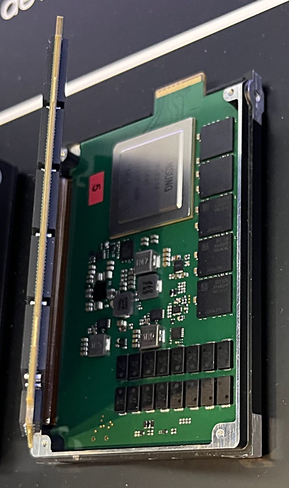
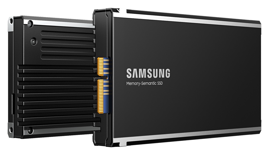
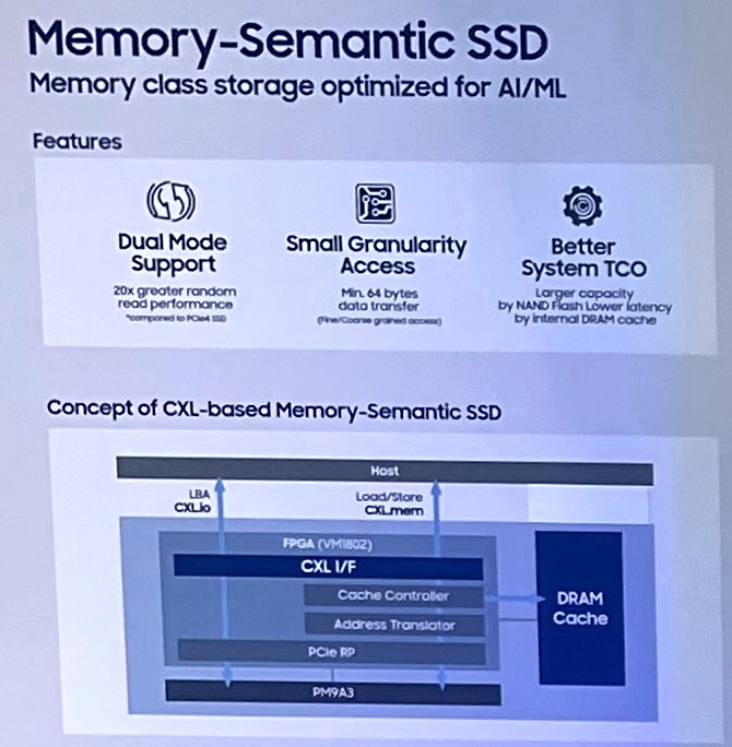
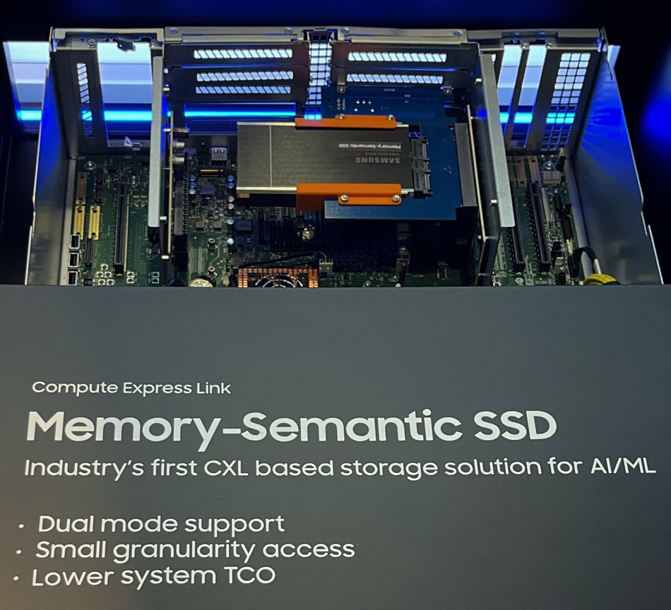
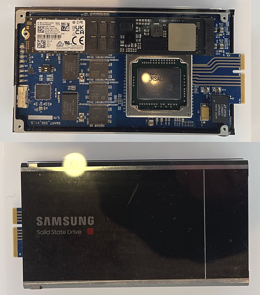
Memory-Semantic SSD
This is a hybrid DRAM and NAND drive supporting PCIe 5 and CXL connectivity with the DRAM providing a cache – 8GB in a canned rolling presentation – which is addressed with load-store memory semantic commands. This gives it superfast speed with a 20x improvement, according to Samsung, in 128 bytes random read IO performance and latency over a PCIe 4 SSD. The drive is targeting AI and machine learning apps that need fast processing of smaller data sets, and real-time RecSys inference application requirements can be met.
The DRAM is a data landing zone and Samsung’s controller copies the data to the NAND. The concept here is to provide equivalent capacity to an all-DRAM config similar performance through the caching but at much lower cost than a DRAM-only set up. It has a minimum 64 bytes data transfer base compared to NAND’s 4KB – according to a Samsung slide.
A booth display diagram indicated that the NAND portion of this drive is Samsung’s PM9A3 – an enterprise PCIe 4 interface SSD. That means the NAND part of this Memory-Semantic Drive provides from 960GB though 1.92TB, 3.84TB, 7.68TB, and 15.36TB of capacity using 128-layer 3D NAND in TLC format. The NAND performance is up to 1,100,000/200,000 random read/write IOPS and 6.95/4.1 GB/sec sequential read/write bandwidth.
So the Memory-Semantic drive is the innards of a PM9A3 front-ended by a CXL interface controller device with a side order of DRAM cache.
Now let’s hit the back of our envelope again and apply the 20x improvement in random read I/O, implying this Memory Semantic drive can hit up to 139GB/sec sequential read bandwidth or 22 million random read IOPS – it depends what Sammy means by random read I/O. Both are hugely impressive numbers.
The dual-mode interface means it be accessed as a NAND SSD with file-based NVME access or as a DRAM with load/store access for memory-mapped files.
A cutaway server showed the drive mounted inside its chassis and it’s obviously not a standard drive format like U.3/2 or one of the EDSFF ones:
We think this should viewed as a prototype drive needing to be sold as a dedicated AI/ML system by a skilled integrator or OEM.
But there’s one more thought: This drive has a CXL load/store interface, is persistent, and is 20x faster than a PCIe 4 SSD. Surely that makes it a candidate for storage-class memory status?
SmartSSD
Sammy’s booth display included a gen-2 SmartSSD, with a PCIe 4×4 interface, AMD Versal FPGA with Arm processor and hardware accelerators, E3 form factor and TP4091(NVMe)/SNIA standardization.
This is a computational storage drive and succeeds the gen-1 version with its PCIe 3 interface and Kintex Ultra FPGA, all in a U.2 form factor. The gen-2 drive case and its printed circuit board look like this:
iPhone camera shot
Telemetry and more
Samsung said it had instrumented its SSD’s NAND, DRAM, controllers and firmware. It has telemetry which provides human-readable metadata about the drive components’ status. This means, Sammy says, datacenters can detect and prevent any potential problems ahead of time.
The company also said that its May-announced UFS 4.0 mobile storage flash for smartphones will enter mass production this month. Two enterprise SSDs are now generally available: the PM1743 PCIe 5 drive and the 24GB SAS PM1653 SSD.
RLHF – From Amazon: Reinforcement learning from human feedback (RLHF) is a machine learning (ML) technique that uses human feedback to optimize ML models to self-learn more efficiently. Reinforcement learning (RL) techniques train software to make decisions that maximize rewards, making their outcomes more accurate. RLHF incorporates human feedback in the rewards function, so the ML model can perform tasks more aligned with human goals, wants, and needs. RLHF is used throughout generative artificial intelligence (generative AI) applications, including in large language models (LLM).
Kioxia exhibited second-generation storage class memory flash at the FMS 2022 event in Santa Clara, with a lower cost per GB than gen 1.
Update. Active plane clarification added to penultimate paragraph. 10 August 2022.
The FL6 storage-class memory SSD from Kioxia is based on first-generation XL-FLASH technology. The storage-class memory was called gen-2 XL-FLASH and, unlike the all-SLC (1 bit/cell) gen 1, this one adds MLC (2bits/cell) NAND to the mix. This enables a die capacity of 256Gbit. Two, four, or eight layers of chips can be stacked in one package.
Curiously, the sample device in Kioxia’s booth bore a Toshiba brand and not a Kioxia one
The MLC addition, it states, “significantly reduces bit cost while providing high performance.” Kioxia provided no performance details but declared that the maximum number of simultaneously operating planes has also increased from the current model, which will allow for improved throughput.
It also said CXL support could be added in the future.
The Toshiba branding was perplexing as the device was exhibited on the Kioxia stand at FMS 2022, but maybe there’s a stock of existing cases.
128 gigabit die (in a 2-die, 4-die, 8-die package);
4KB page size for more efficient operating system reads and writes;
16-plane architecture for more efficient parallelism;
Fast page read and program times – XL-FLASH provides a low read latency of less than 5 microseconds, approximately 10 times faster than existing TLC;
We thought that the gen-2 XL-FLASH could have 32 planes, but we were wrong as a Kioxia spokesperson said: “The number of active simultaneous planes in BiCS5 XL-FLASH has increased from 4 to 8. The total number of planes for both generations is 16.”
We also think that there could be a successor to the FL6 – the FL7 perhaps – built using gen-2 XL-FLASH. In fact we would put money on that.
Western Digital’s latest quarterly revenues dropped 8 percent year-on-year due to falling PC and consumer disk drive purchases – and the storage giant is forecasting 26.7 percent weaker revenues for next quarter, meaning the business situation is worsening.
Revenues in the fourth quarter of WD’s fiscal 2022 ended July 1, were $4.53 billion ($4.9 billion in Q4 fy2021) with a profit of $310 million, lower than a year ago by 52 percent. Full year revenues were $18.8 billion, 11 percent up on the year, with a profit of $1.5 billion, 82.7 percent higher than the prior year.
It was a good year spoiled by a poor final quarter.
CEO David Goeckeler said: “I am proud of our team for driving strong fiscal year 2022 performance, during which revenue grew 11 percent and non-GAAP EPS increased 81 percent, demonstrating progress in unlocking the earnings potential of our business. … The combination of our innovation engine and the multiple channels to deliver our products to the market puts Western Digital in a great position to capitalize on the large and growing opportunities in storage ahead even in the midst of macro dynamics weighing on near-term demand.”
We understand the revenue drop was due to pandemic effects, the Ukraine-Russia war and supply chain issues, compounded by inflation and recession fears holding back consumer spending.
WD generated $295 million in cash flow from operations, made a scheduled and discretionary debt repayment of $150 million and ended the quarter with $2.33 billion of total cash and cash equivalents. Gross margin was 31.9 percent, up 0.1 percent on the year. EPS was $0.95, down 52 percent annually.
The Q4 segment results:
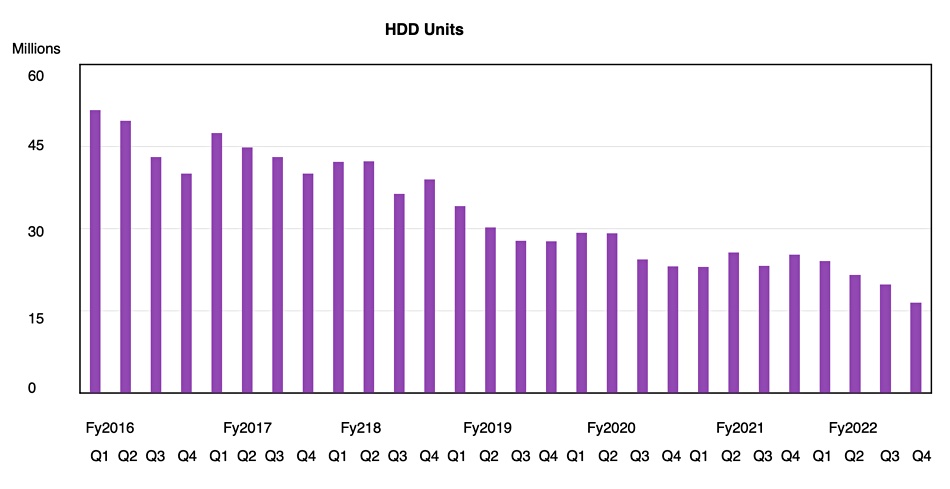
HDD Units: 16.5 million, down 34.8 percent annually
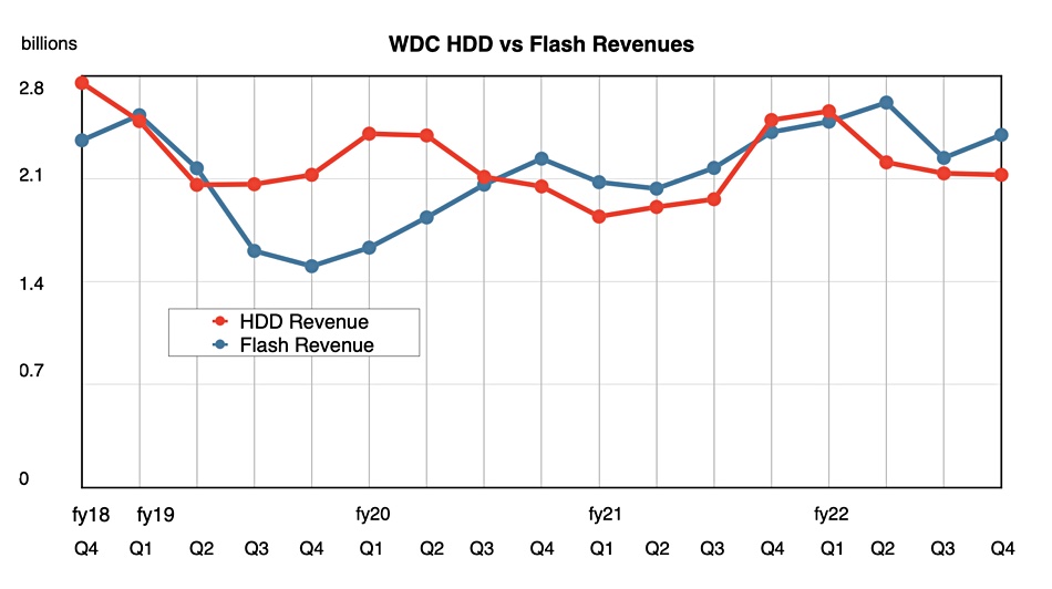
HDD revenues: $2.13 billion, down 14.9 percent
Flash/SSD revenues: $2.4 billion, down just 0.8 percent
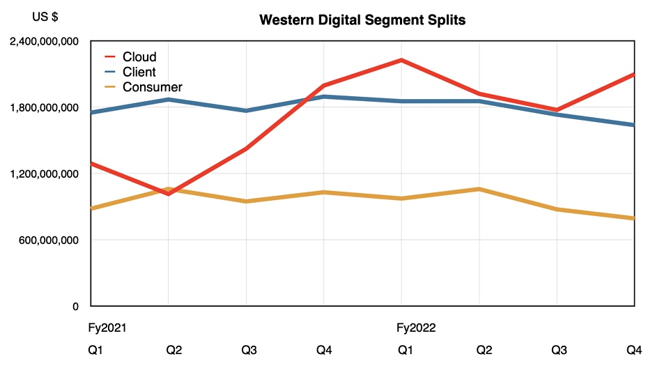
Revenue by end-market:
Cloud (hyperscalers): $2.1 billion, up 5 percent
Client: $1.64 billion; down 14 percent and 36 percent of revenues
Consumer: $793 million; down 23 percent; now just 18 percent of revenues
Cloud has becoming the dominating market segment in WD’s market segment revenue mix.
Customers bought fewer desktops and notebooks with disk drives, and fewer retail disk drives as well. Wells GArgo analyst Aaron Rakers told subscribers: “The y/y decline was driven by broad-based retail weakness across both HDD and flash products.”
But the hyperscalers bought more nearline disk drives and they had more capacity than a year ago, with WD shipping a total of 111 EB to cloud customers in the quarter. The average selling price per disk was up by nearly a quarter on the year, at $120, reflecting the increased disk capacity.
WD disk drive unit ship history. Capacity increases have sent exabyte shipments up and held HDD revenues steady-ish (see chart below) while the unit numbers have trended down.
WD said it was ramping a second cloud customer with SMR (Shingled Magnetic Recording) disk technology this quarter and is on track to lead the industry’s transition to SMR based drives for the cloud.
WD’s flash/SSD revenues overall were flattish; down just 0.8 percent. Enterprise SSD revenue more than doubled sequentially in the quarter and rose 38 percent annually. Gaming exabyte shipments grew nearly 70 percent year-over-year.
We expect WD’s flash/SSD revenues to slowly edge ahead of HDD revenues over the next few quarters.
The outlook for next quarter’s revenues is $3.7 billion plus/minus $10 million; down a huge 26.7 percent year-on-year. This surprisingly weak guidance sent the share price down 8.8 percent, from $50.02 to $45.63, in early post-results trading. Rakers said: “WD expects Flash to lead its F1Q23 q/q rev. decline while HDD rev. is expected to decline modestly…. WD’s significantly weaker outlook reflects deteriorating consumer & client (PC) demand.”
Netlist, which builds NVDIMMs and other memory modules, is suing Google, Samsung and Micron for patent-related violations and hoping to gain licensing fees in the millions – if not tens of millions or higher. And it has just won a waystation victory.
The financial prospects are so great that a Seeking Alpha pundit has called it the lawsuit of the century.
Netlist has a history of making memory-type products and then suing businesses it thinks ripped off its patent ideas or broke cross-licensing deals. For example, in 2017 it was pursuing Diablo Technology over wrongly using its patented NVDIMM tech – up to the point where Diablo collapsed and ceased trading.
Netlist also sued SK hynix for breaking its patents and received around $40 million from hynix in a cross-licensing deal in April last year.
The waystation victory was against Samsung, but involves Google as well. The Micron suit is a separate issue.
Background
Back in 2009, Netlist sued Google in a Delaware court, and said that Google had wrongly used Netlist-patented IP – specifically US Patent No. 7,619,912 or the ‘912 patent, which refers to the use of rank multiplication in an LRDIMM (Long Range DIMM) memory module. Such DIMMs can have four ranks or blocks of memory, and the patent describes IP to present the LRDIMM logically as only having two ranks, thus getting over system memory controller limits on the maximum rank count.
Agni Research explained “Netlist asserts that the ‘912 patent enabled Google to build servers with high capacity and rapid memory that allowed said servers to store an entire Oracle database in memory which allowed lightning-fast search results. The ‘912 patent played a large part in Google’s dominance in search.”
Google contested the validity of the ‘912 patent and, after nine years of legal disputation, the US Court of Appeals upheld a prior decision that the patent was valid.
While this was going on, Netlist had set up a cross-licensing deal with Samsung over the use of its technology. Later it decided Samsung broke the contractual terms of the deal and sued in 2020 for breaking the deal terms, again for patent infringement and, then it suspended the cross-licensing deal.
Samsung defended its corner and counter-sued Netlist. Earlier this year, on February 18, Netlist won a victory against Sammy, as the court said the Korean giant had broken the cross-licensing deal terms and Netlist was entitled to suspend the contract. It then pursued Samsung for patent infringement in a Texas court.
Keep this in mind as we move on to May 5 this year, when Netlist’s lawyers gained a court decision in their favor in the Google case. This, they said, meant Google had used Netlist IP wrongly and was responsible for the patent infringement. Netlist could then legally chase Google for recompense.
That lawsuit was stayed (paused) for 90 days on July 13 with the judge deciding that, as Samsung had supplied the patent-infringing memory modules to Google, things could wait while the court in the Netlist-Samsung case decided if Samsung had violated Netlist’s patent.
Now, finally, we come to the latest judgement – a waystation judgement as we term it, because it is just a waystation on a multi-year legal odyssey. Samsung had filed an amended complaint against Netlist which Netlist had moved to dismiss. That motion was granted, in part, with the court saying Samsung could not file a second amended complaint; that door was closed.
Netlist says that “The partial dismissal means Samsung cannot pursue a separate action on the patents Netlist first asserted in Texas, and now cannot carry out its alleged obligation to protect Google from the ‘912 Patent in Delaware.”
So, the Netlist court victory against Samsung is a waystation on its road to suing Google and, it hopes, getting mucho licensing revenue, and maybe damages, from Google – as well as licensing revenue from Samsung.
The Micron case
This completely separate litigation involves Netlist asserting that Micron infringed its patented RDIMM and LRDIMM technology – including the ‘912 patent – by shipping product and not agreeing to a requested licensing agreement. This case started earlier this year and is currently open with no judge assigned.
Seeing a 128TB Samsung SSD using QLC (4bits/cell) flash got me thinking abut a PLC (5bits/cell) version which could have a 150TB or so capacity. Imagine 32 of these (in long ruler format) put in a 1RU chassis, giving us a 4.8PB box. Now take another step forward and put 40 of these chassis in a rack to produce a 192PB vault. Compress and dedupe it 3x and we have a 576PB box – slightly over half an exabyte.
Update. Comment added from Nimbus CEO Thomas Isakovich. 10 August 2022
It would be pretty useless, as the power budget would probably blow past a 15KW rack limit. So you could only use it if most of the drives were inactive – like in an archive scenario where the bulk of the drives are on standby until you need to read their data. Data is streamed in and written infrequently and you could have an SLC (1bit/cell) landing zone for that to speed things up. Have we just invented an all-flash archive?
It would have an access speed many times that of tape and would be an active all-flash archive.
A Quantum i6H Scalar tape library rack can hold, we estimated, 14.4PB uncompressed and 36PB of compressed data using LTO-9 tapes. Our imagined archive AFA could store 576PB – 16 times more.
The PLC flash has a very short endurance compared to QLC – say sub-500 cycles. That makes it useful for SD cards for cameras, camcorders and USB sticks, but not for enterprise mixed read-write use. But read-intensive use is another matter, especially when the actual read rate is liable to be low anyway. As a write-once-read-many (WORM) technology, PLC flash makes sense.
Discussing this with analyst Chris Evans, we realized that, in fact, with an SSD’s quite low idle state power draw then you could have a rack-full of drives and not exceed the rack’s power budget – so long as software managed the overall power draw by limiting the number of drives active at any one time. In effect we would have the flash equivalent of the old Copan MAID disk drive array concept – a massive array of inactive drives.
If an analyst and I can come up with this idea during a coffee break at the Flash Memory Summit, then engineers at the the solid state drive manufacturers got there months ago. If the idea really has legs – price/performance/power budget/access speed legs – then we might see the first flickers of light about it emerging from the darkness of the solid state product development jungle in the next few months.
Or perhaps this is all a flash fantasy and will get nowhere.
Nimbus comment
Nimbus CEO Thomas Isakovich contacted us to say: “This achievement (a flash-based exascale data vault) was my motivation when designing our ExaDrive 3.5” SSD. To achieve this, one must re-think the goals and priorities:
Focus on power efficiency, capacity, and cost, not IOps, GBps, or DWPD à go with SATA and QLC, which offer lower power and lower cost than NVMe/TLC and adequate performance
Leverage existing density-optimized enclosures à go with 3.5” top-loading enclosures that have unmatched volumetric rack density and a healthy and competitive ecosystem
Your idea is not fantasy – in fact, it is quite a reality today with ExaDrive:
Using ExaDrive 64 TB QLC SSDs achieves 1.5 PB per U raw today (using 90 or 100 slot 4U enclosures today from multiple vendors), or about 68 PB raw capacity per 44U rack.
With 5:1 compression/dedupe, and accounting for SSD fault redundancy, that’s 335 PB usable per rack, or a whopping 1 exabyte usable in just 3 racks.
Power (due to our patented SATA/QLC ExaDrive controller) is a low 20 kW per rack, easily achievable in today’s datacenters, which equals a mere 0.06 watts per usable TB.
Note that our approach is based on an industry-standard drive form factor and interface, not a proprietary flash module/blade
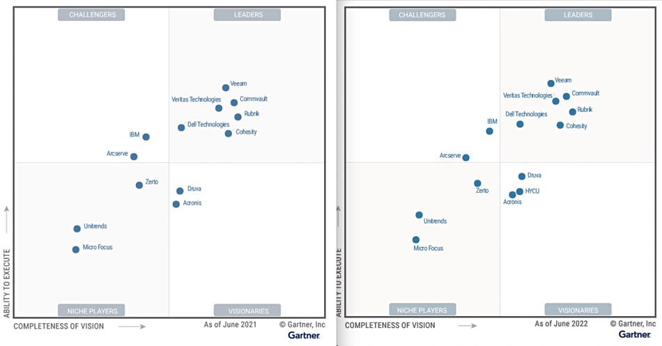
It’s near quadratic equality with just minor changes in the 2022 Gartner Backup and Recovery Magic Quadrant. The only new entrant is HYCU, hustling in for the first time as a Visionary.
Enterprise backup and recovery software systems are, according to Gartner’s definition, “designed to capture a point-in-time copy (backup) of enterprise workloads in on-premises, hybrid, multicloud and SaaS environments and write the data to a secondary storage target for the purpose of recovering this data in case of loss.”
Commvault leads the rankings, closely followed by Veeam and Rubrik with Veritas in hot pursuit, followed by Cohesity also in close pursuit, and then Dell a little way behind. We note that Rubrik has been ranked as having the most Completeness of Vision and Veeam has the highest Ability to Execute, while Commvault has the strongest balance between these two measures.
This is a remarkably stable MQ in some ways. For example, Veritas says this marks its 17th time being named a Leader and Commvault has been named a Leader for the 11th consecutive year. Veeam has been positioned as a Leader for the 6th consecutive year.
If we compare the latest MQ with the year-ago quadrant we can see that very little has changed – apart from HYCU’s entrance. Oh, and both Challenger IBM and Visionary Druva have moved some way closer to the Leaders’ quadrant.
The main event is HYCU’s arrival on the MQ scene. A HYCU spokesperson told us: “Everyone here is pretty excited. As a first-time entrant we are a Visionary. … And, as Gartner noted in our strengths, it’s in large part due to our ease of use, multicloud and hybrid cloud support and deep Nutanix integration.”
Scanning through the MQ authors’ comments about the vendors we found interesting snippets.
Acronis – “During the evaluation period … opened 12 new datacenter locations. … Acronis offers a strong and differentiated data protection solution for remote sites/edge locations and endpoints localized in more than 25 languages.”
Arcserve – “During the evaluation period, Arcserve merged with StorageCraft, launched new N Series Appliances based on Nutanix, expanded UDP appliance capacity to 1PB, released new Arcserve SaaS Backup via OEM agreement with Keepit, and released UDP 8.1, which includes support for Oracle Standard Edition and multifactor authentication.”
Unitrends – “In the last 12 months, Unitrends released ten software updates from version 10.5.3 through 10.6.2.”
Veeam – “In the last 12 months, it released 30 product updates as well as plug-ins for eight OEM partners.”
Vendors updated and extended their products at vigorous rates and still their MQ position didn’t change. The general rate of development is so high that it didn’t count much at all. What do you have to do to improve your position in this MQ – to really move the needle around the dial?
Download the full report here. This provides Gartner’s comments on the strengths of, and challenges faced by, each supplier in the MQ.
Bootnote
The Gartner Magic Quadrant is a 2-axis chart with Ability to Execute being the vertical axis and Completeness of Vision the horizontal one. There are four subsidiary quadrants or squares: Challengers and Leaders in the top half of the chart and Niche Players and Visionaries in the bottom. The balance between execution and vision is provided by closeness to a non-shown bottom left to top right diagonal line.