


Startup Enfabrica, which is developing an Accelerated Compute Fabric switch chip to combine and bridge PCIe/CXL and Ethernet fabrics, has raised $125 million in B-round funding.
Its technology, which converges memory and network fabric architectures, is designed to bring more memory to GPUs than current HBM technology using CXL-style pooling, and to feed data into memory through a multi-terabit Ethernet-based switching scheme. This relies on the ACF-S chip, under development, and 100-800Gbps Ethernet links.

CEO and co-founder Rochan Sankar stated: “The fundamental challenge with today’s AI boom is the scaling of infrastructure… Much of the scaling problem lies in the I/O subsystems, memory movement and networking attached to GPU compute, where Enfabrica’s ACF solution shines.”
The funding round was led by Atreides Management with participation from existing investors Sutter Hill Ventures, Valor, IAG Capital Partners, Alumni Ventures, and from Nvidia as a strategic investor. Enfabrica’s valuation has risen 5x from its 2022 $50 million A-round valuation.
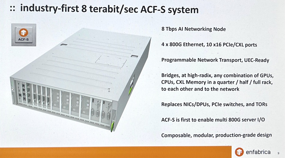
Enfabrica is developing an 8Tbps switching platform, enabling direct-attach of any combination of GPUs, CPUs, CXL-attached DDR5 memory, and SSD storage to high-performance, multi-port 800-Gigabit-Ethernet networks. It has around 100 engineers building chips and software, based in Mountain View, CA, Durham, NC, and Hyderabad, India.
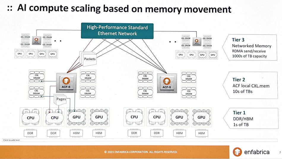
It sees memory in terms of tiers. DDR and HBM forms the fastest layer with single digit terabyte capacities. Tier 2 is CXL memory local to the ACF-S device, and comes in the tens of terabytes. Networked memory accessed by RDMA send/receive is tier 3 and has thousands of terabytes of capacity. ACF-S-connected memory can be composed for specific workloads as needed.
The company has proved that its switch chip architecture and design is correct and should accelerate data delivery to GPUs as intended. The VCs have been convinced by its progress so far and now it has funding to build it. Sankar said: ”Our Series B funding and investors are an endorsement of our team and product thesis, and further enable us to produce high-performance ACF silicon and software that drive up the efficient utilization and scaling of AI compute resources.”
Enfabrica thinks that its technology is especially suited to AI/ML inference workloads, as distinct from AI/ML training. Sankar said that current training systems gang together more GPUs than are needed for compute just to get sufficiency memory. According to Sankar, this means the GPUs are under-utilized and their expensive processing capacity is wasted.
The ACF-S chip and allied software should enable customers to cut their cost of GPU compute by an estimated 50 percent for LLM inferencing and 75 percent for deep learning recommendation model inferencing at the same performance point. This is on top of interconnect device savings as the Enfabrica scheme replaces NICs, SerDes, DPUs, and top-of-rack switches.
ACF switching systems with Enfabrica’s ACF-S silicon will have 100 percent standards-compliant interfaces and Enfabrica’s host networking software stack running on standard Linux kernel and userspace interfaces.
Sankar confirmed that the Enfabrica technology will be relevant to high-performance computing and little development will be needed to enter that market. Enfabrica could, in theory, support InfiniBand as well as Ethernet, but sees no need to do so.
Customers can pre-order systems by contacting Enfabrica.
Bootnote
A SerDes is a Serializer Deserializer integrated circuit device which interconnects single line parallel and serial network links. The Serializer or transmitter converts parallel data to a serial stream, while the Deserializer or receiver converts serial data to a parallel stream.


