


SK hynix has unveiled a sample 321-layer 3D NAND chip and is in the process of developing a PCIe gen 5 interface for UFS flash modules.
At FMS 2023 in Santa Clara, the company showcased its 321-layer flash chip, noting it offers a 1 terabit capacity using the TLC (3bits/cell) format. This layer count surpasses previous benchmarks set by Micron’s 232 layers and Samsung’s 236 layers, while Kioxia and WD currently have technology at the 218-layer level. YMTC’s in-development 232-layer chip is delayed due to US tech export restrictions.
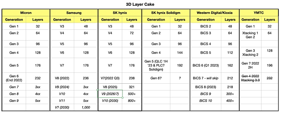
SK hynix said: “With another breakthrough to address stacking limitations, SK hynix will open the era of NAND with more than 300 layers and lead the market.” The new chip is projected to enter mass production in the first half of 2025, indicating it’s in the early stages of development.
While specifics are unclear, there’s speculation on whether the 321-layer chip consists of two separate 260-layer class chips (string stacking) or is a singular stacked device, which would pose more manufacturing challenges. Given that the SK hynix 238-layer chip is a combination of two 119-layer components, a string stacking technique seems plausible.
Earlier this year, SK hynix presented on its 300+ layer technology at the ISSCC 2023 conference, boasting a record 194GBps write speed. A white paper released at the time stated: “To reduce the cost/bit, the number of stacked layers needs to increase, while the pitch between stacked layers decreases. It is necessary to manage the increasing WL (wordline) resistance produced by a decreased stack pitch.”
No technical details are included in its latest announcement.
SK hynix’s existing 238-layer generation features a 512Gb die, but with the increased density of the 321-layer technology, this will be expanded to 1Tb. This suggests potential for greater storage capacities within compact spaces for SSDs, as well as embedded UFS-type NAND drives for mobile devices and lightweight notebooks.
SK hynix also announced its introduction of a UFS v4 chip, offering transfer speeds up to 5,800 MBps, with a UFS v5 variant, capable of up to 46.4Gbps transfer speed, currently in the works.
It is also progressing towards the development of PCIe gen 6 interface drives, offering an 8GBps lane bandwidth, a significant leap from PCIe gen 5’s 4GBps. This development, in conjunction with SK hynix’s UFS advancements and the 321-layer technology, is attributed to the rising demand from AI workloads, notably influenced by platforms like ChatGPT and other large language models.
Jungdal Choi, head of NAND development at SK hynix, said: “With timely introduction of the high-performance and high-capacity NAND, we will strive to meet the requirements of the AI era and continue to lead innovation.”


