


Mountain View-based Enfabrica has raised $115 million in C-round funding and says it will ship its 3.2 Tbps Accelerated Compute Fabric (ACF) switch chip in Q1 2025.
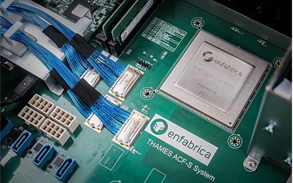
The ACF-S superNIC switch combines PCIe/CXL and Ethernet fabrics to interconnect GPUs and accelerators with multi-port 800-Gigabit-Ethernet connectivity.
Enfabrica raised $125 million in September 2023 for this work. The new funding takes its total raised since it was founded in 2019 to $290 million. Spark Capital led this latest oversubscribed equity financing round with new investors Arm, Cisco Investments, Maverick Silicon, Samsung Catalyst Fund, and VentureTech Alliance. Existing investors including Atreides Management, Alumni Ventures, IAG Capital, Liberty Global Ventures, Sutter Hill Ventures, and Valor Equity Partners participated as well.

Enfabrica CEO Rochan Sankar stated: “We were the first to draw up the concept of a high-bandwidth network interface controller fabric optimized for accelerated computing clusters. And we are grateful to the incredible syndicate of investors who are supporting our journey. Their participation in this round speaks to the commercial viability and value of our ACF SuperNIC silicon. We will advance the state of the art in networking for the age of GenAI.”
The new cash will be used to drive ACF’s volume production ramp, grow Enfabrica’s global R&D team, and expand its next-generation product line development.
The ACF-S (switch) chip has high-radix, high-bandwidth, and concurrent PCIe/Ethernet multipathing and data mover capabilities. Enfabrica claims this is four times the bandwidth and multipath resiliency of any other GPU-attached network interface controller (NIC) product in the industry. And it says this level of data movement is demanded by the large-scale training, inference, and retrieval-augmented generation (RAG) workloads associated with the latest AI models.
It offers full-stack operator control and programmability, integrating software-defined networking (SDN) with remote direct memory access (RDMA) networking, which it says is widely deployed in AI datacenters. The switch has 800, 400, and 100 GbE interfaces, a high radix of 32 network ports, and 160 PCIe lanes on a single ACF-S chip. The term “radix” refers to the number of ports or connections a switch can support.
Enfabrica says the switch can be used to build AI clusters of more than 500,000 GPUs, from multiple vendors, with an “efficient two-tier network design, enabling the highest scale-out throughput and lowest end-to-end latency across all GPUs in the cluster.” The ACF-S software supports standard collective communication and RDMA networking operations through a consistent set of libraries compatible with existing interfaces. The RDMA networking is software-defined.
The ACF-S has Resilient Message Multipathing (RMM) technology, which “boosts AI cluster resiliency, serviceability, and uptime at scale” and “eliminates AI job stalls due to network link flaps and failures to improve effective training time and GPU compute efficiency.”
It also features Collective Memory Zoning, which provides “low latency zero-copy data transfers, greater host memory management efficiency and burst bandwidth, and higher system resiliency across multiple CPU, GPU, and CXL 2.0-based endpoints attached to the ACF-S chip.” This increases the efficiency and overall Floating Point Operations per Second (FLOPs) utilization of GPU server fleets.”
B&F understands that Enfabrica’s switch is intended for use in large-scale GPU clusters, which are currently built by hyperscalers such as the big public clouds, Meta, xAI with Colossus, other large language model developers like OpenAI, and GPU server farm suppliers such as CoreWeave. It’s a relatively limited number of customers who will need to buy thousands of Enfabrica’s chips if it is to succeed.
Nvidia interconnects its GPUs with NVLink, providing up to 1.8 TBps of bidirectional bandwidth. Enfabrica is GPU vendor-agnostic. The NVLink-C2C (Chip-to-Chip) extension supports CXL, meaning Enfabrica is betting that its technology can be used outside an all-Nvidia environment. That environment in the GenAI world is practically nonexistent today, but hyperscalers like Google, AWS, and Azure are developing their own GPU-like accelerators.
Sankar said: “Our ACF SuperNIC silicon will be available for customer consumption and ramp in early 2025. With a software and hardware co-design approach from day one, our purpose has been to build category-defining AI networking silicon that our customers love, to the delight of system architects and software engineers alike. These are the people responsible for designing, deploying and efficiently maintaining AI compute clusters at scale, and who will decide the future direction of AI infrastructure.”


