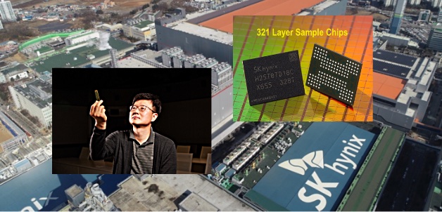
SK hynix has started mass producing its 321-layer 3D NAND, winning the flash layer count race, which Western Digital has claimed to be over with its 218-layer NAND.
The Korean NAND fabber is using a so-called three-plugs technology to interconnect a triple stack of layered NAND, each stack being around 100 layers, and build a 1 Tbit TLC (3 bits/cell) chip. It sampled the 321-layer chips in August last year.
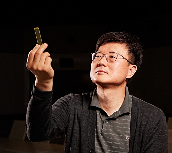
Jungdal Choi, head of NAND development at SK hynix, reckons: “SK hynix is on track to advancing to the Full Stack AI Memory Provider by adding a perfect portfolio in the ultra-high performance NAND space on top of the DRAM business led by HBM (High Bandwidth Memory).”
SK says its plugs complete the NAND cell production process initiated by stacking substrates layer by layer. It says “repeating the cell formation process for each layer would be inefficient and increase manufacturing costs. Therefore, multiple layers of substrate are first stacked, then vertical holes called plugs are drilled through the layers before cells are formed next to the holes.”
The holes are not drilled but etched. Other NAND manufacturers call these holes Through Silicon Vias (TSVs). The etching equipment works well up to 100 layers but then becomes unreliable. Instead it creates the plugs in three sets of 100 layers, which are stacked vertically.
It says that with its three-plugs technique, “all the processes, including cell formation, can be performed simultaneously on all layers.”
“With this, SK hynix was able to conduct a single process to simultaneously fabricate the key structures – word lines and word line staircases – that apply voltage and the passageways for electrons.”
Word lines are the connections that bind the control gate of each layer of NAND cells. A word line staircase is a structure for exposing the word line of each layer to the top surface.
The plugs in each layer, however, may not be perfectly aligned.
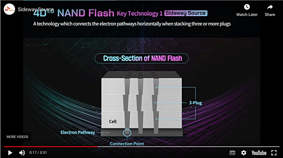
SK hynix has another technology trick up its sleeve here. The plug is lined with CTF (Charge Trap Flash) film and this needs to be removed at the bottom where it meets an electrical pathway. This is called the connection point in the diagram above. The CTF film is a composite of oxide and nitride films that replaces a floating gate.
The company says: “Previously, etching gas was injected from the top of the plug to vertically remove the CTF film at the bottom of the plug. However, when stacking two or more plugs, the centers of the plugs were not aligned. This prevented the etching gas from reaching the bottom, damaging the CTF film on the side of the plug that serves as a cell.”
It solved this problem by providing a separate sideways source path for the etching gas. “The etching gas is injected into a separate pathway to reach the bottom of the NAND layer and remove the CTF film on both sides of the plug. With Sideway Source technology, the etching gas is not directly injected into the plug. Therefore, even if the plugs are misaligned, the interior remains undamaged. As a result, SK hynix has significantly reduced its defect rate, increased productivity, and addressed the problem of increased costs associated with multiple stacking.”
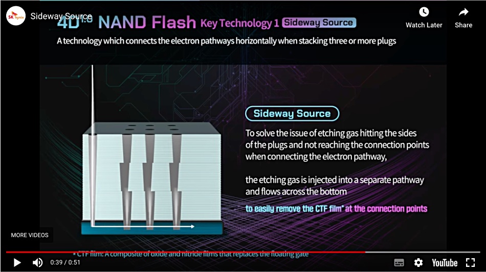
The horizontal pathway connections leave no voids at the bottom of the NAND layer.
SK hynix is emphasizing NAND performance. With 321-layer technology, it can match the capacities its competitors reach with QLC (4 bits/cell) chips using lower 3D NAND layer counts, and get faster than QLC performance and endurance with its TLC (3 bits/cell) formatting.
The company says this “latest product comes with an improvement of 12 percent in data transfer speed and 13 percent in reading performance, compared with the previous generation. It also enhances data reading power efficiency by more than 10 percent.” SK hynix sees its 321-layer NAND suited for AI applications needing low power and high performance.
Wedbush analyst Matt Bryson tells subscribers: “While the layer count is certainly impressive, we have encountered less promising feedback around the expected quality of Hynix’s new parts, with our conversations suggesting Micron and Kioxia/WD (with BiCS8) appear to be leading in anticipated next generation NAND bit performance.”
SK hynix said its 321-layer NAND chips will be available to customers in the first half of 2025.


