

Micron’s NVDRAM chip could be a proving ground for technologies used in other products – and not become a standalone product itself.
The 32Gb storage-class nonvolatile random-access memory chip design was revealed in a Micron paper at the December IEDM event, and is based on ferroelectricRAM technology with near-DRAM speed and longer-than-NAND endurance. Analysts we have spoken to suggest this chip may not become a commercial product in its own right. Instead its component technologies could be used in other products.
Update. Additional Jim Handy thoughts added below, 16 Jan 2024.
Update. Jim Handy notes on NVDRAM refresh added. 18 Jan 2024
Industry view: Objective Analysis

Jim Handy from Objective Analysis reckons ”Micron’s device introduced three interesting new technologies.” We’re told those three are:
- A ferroelectric capacitor that’s smaller than the capacitors used in today’s DRAM. This technology has only previously been used in experiments.
- A vertical transistor with a polycrystalline silicon channel. 3D NAND typically uses an amorphous channel, which is easier to produce. Micron’s one starts with a similar amorphous channel and then uses a laser anneal step to crystallize the channel.
- It stacks the DRAM in a back-end process, and uses CUA (CMOS Under Array) for the support logic to make the die area very small. CUA is a technology pioneered by Micron with some of its first 3D NAND, and which has now been adopted by all leading NAND flash makers.
Handy told us: “All of this allowed Micron to make a 32Gb chip with a reasonable area of 71mm² using a 48nm process, which is enormous by today’s DRAM standards.”
Samsung produced the world’s first 32Gb DDR5 DRAM die in September last year, using a 12nm-class production process, four times smaller than Micron’s NVDRAM process.
Overall, the ferroelectric capacitor and the polycrystalline silicon channel are the standout technologies in Micron’s NVDRAM, Handy said.
NAND, whether planar or 3D, does not use capacitors to hold information, but DRAM does. DRAM stores binary data as electric charge in arrays of capacitors that need constant refreshing – or else the charge leaks away and the data is lost; it is volatile. DDR2 SDRAM chips support a maximum of 64ms between refresh cycles. DDR5 and LPDDR5 have a shorter 32ms refresh period.
A ferroelectric capacitor does not store electric charge. Instead it stores data using the electric polarity of zirconium or titanium atoms in octahedron crystals of lead and oxygen, for example. This mechanism is stable and only needs refreshing when the ferroelectric capacitor is read.
According to Handy, Micron’s FeRAM uses hafnium oxide with zirconium doping. He said: “I suspect that all DRAM companies are investigating it since it has a very high dielectric constant that can be used to shrink the cell capacitor.”
When DRAM capacitors shrink below a certain size they lose the ability to reliably store electric charge, and are made tall while being narrow to decrease a DRAM cell’s size in two dimensions while still functioning. If they could have a lower vertical height as well then their overall size would shrink further, allowing increased density (and thus memory capacity) on a die.
Handy says hafnium oxide “allows refresh rates to be reduced to five percent of a standard DRAM’s under heavy use, and to well below one percent when lightly used. Such low refresh requirements will provide a significant reduction in power consumption which is of the utmost importance to hyperscale data centers. I would suspect that DRAM makers are being given great encouragement to experiment with hafnium oxide capacitors.”
We understand that heavy and light use here refers to the read rate, with every read needing to be followed by a refresh. If there’s no read operation, there’s no need to refresh, and so it should be stable, one would think. Handy is not so certain about this: “This is one of the points that the paper doesn’t describe well … In some places the authors say that it’s nonvolatile, and in others they talk about having lower refresh requirements.”
He tells us that he has heard hints “that the chip that Micron presented is not slated for production, but I would expect for one or more of these technologies to make its way to use.” He enlarges on this: “What we don’t know is how this chip’s production cost and yield compare against today’s DRAMs. If there’s a path to improved profitability, then Micron will adopt it.”
Handy also said: “Way back in the late 1990s I coauthored a paper for Gartner Dataquest, where I worked at the time, saying that DRAM was likely to move to ferroelectric capacitors. It didn’t happen then, but it seems to be happening now. I know that Intel presented a paper at IEDM 2020, I think, that showed a four-layer 3D DRAM made using a hafnium oxide dielectric simply to get the capacitor smaller.”
Industry view: MKW Ventures

Analyst Mark Webb, of MKW Ventures, was director of manufacturing for the NVM Solutions Group at Intel Corporation from 2008 to 2012. He says the NVDRAM chips Micron “demonstrated are very complete and the data looks good. Micron spent a lot of time and energy on this program.”
Webb sees two reasons “why detailed technical papers like this are published at IEDM by a major company.” They are:
- The product is ready to go and products are announced in parallel with the paper.
- The product or project has been cancelled for some reason not in the paper.
His conclusion is that: “After reviewing the data, we do not expect this particular version to progress to an actual product.”
That concurs with the hints that Handy referred to.
We have asked Micron for an NVDRAM briefing and that request is being considered by the manufacturer.
B&F understands that future 3D DRAM technologies may use hafnium-oxide-based capacitors and so enable increased density and substantially lower electrical power use.
Bootnote
Objective Analysis has more information on hafnium oxide FeRAM in its Emerging Memories Branch Out report.
Update
Jim Handy told us: “The point of Micron’s ferroelectric capacitor is to be nonvolatile. It seems that there’s no die size penalty to go nonvolatile, so that’s the route they took. If this ends up being a production-worthy technology, then NVDRAM could displace DRAM very rapidly, and would be a good candidate for 3D DRAM as well.”
He added: “I would doubt that Micron would have gone as far as to develop a 32Gb chip had they not originally intended to commercialize it. Chips that are made to prove out a technology are rarely designed with aggressive bit densities. That would just make the designer’s job a lot more difficult. I would expect for aspects of this chip to appear in a commercial product in the next few years.”
NVDRAM refresh update
Jim Handy emailed us about the concept of NVDRAM refreshes, saying: “My confusion has been about how to interpret the IEDM paper’s Figure 14, which shows how much overhead is consumed by refreshes and RFM. (Since the NVDRAM is on this chart, I misunderstood to think that it must somehow need refreshing.)”
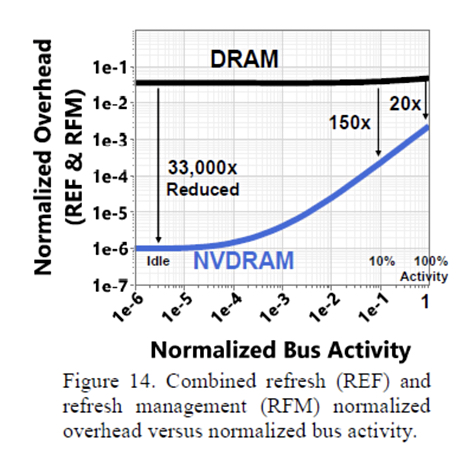
As NVDRAM is, by definition, non-volatile, it should not need refreshing. However there are circumstances in which a refresh is necessary, as Handy explains. The IEDM paper’s Fig 14 is shown right for reference.
“REF is simply standard DRAM refresh, which Micron tells me NVDRAM doesn’t need. RFM is a new DDR5 command that helps combat DRAM rowhammer attacks by performing a refresh on a row and its adjacent rows. The system is expected to issue RFMs more frequently when there’s been unusually high activity in the adjacent rows (i.e. they are being “hammered” on.) This activity could stem from high bus utilization, or from an attack. When in doubt, issue an RFM. NVDRAM would use this kind of refresh as a defense against rowhammer attacks.
“It seems that the bulk of the activity that drives Figure 14’s NVDRAM line consists of RFM commands, although there may also be some MM (Memory Management) activity in there, too. MM is a proprietary command that Micron has created just for the NVDRAM. They’re not explaining any more than that. Since MM doesn’t appear on the vertical axis, it’s fair to assume that Micron is not including any MM activity in this chart.
“NVDRAM, doesn’t use REF at all, so the shape of the NVDRAM line would tell us that there’s an increasing amount of RFM overhead as bus activity increases.
“The Standard DRAM line at the top is nearly flat because DRAM always needs to be refreshed every 64ms (or whatever the specification calls for) no matter how active the bus is. As with the NVDRAM, RFM must be invoked more often when there are more row activations, but its contribution to the overhead is so small (compared to REF) that doesn’t have any real impact on the DRAM line until the very right side of the curve.
“I would suspect that the RFM-alone curve for DRAM, if you were to remove all REF, would look almost identical to that of the NVDRAM.”


