


Micron has revealed a substantial interest in Ferro-electric RAM (FeRAM) technology with a paper presented at the December 2023 IEDM event. This could be its Optane storage-class memory replacement.
We briefly mentioned Micron’s latest FeRAM activity in a Storage Ticker roundup and will look at it in more detail here, with three items in mind. What is FeRAM? Where does it fit in the memory market? What are Micron’s prospects?
FeRAM tutorial
Ferro-electric RAM is a non-volatile random-access memory that stores binary data as an electric polarity in a dipole in a ferro-electric capacitor, generally composed of Lead Zirconium Titanate (PZT). The dipole polarization direction (P positive or P negative) is caused by the movement of a zirconium (Zr) or titanium (Ti) atom (cation) in lead (Pb) and oxygen perovskite crystals making up the capacitor. There are two stable crystal states, notionally with the Zr or Ti atom up or down from a charge center. The position can be discerned as a difference in voltage and that indicates a binary 1 or 0. The up or down polarization stays constant when the electric field is removed.

The polarity state is changed by applying a specific voltage to the ferroelectric capacitor. It is not changeable by magnetism or external radiation. The capacitor is not made of iron and so the ‘ferro’ part of the name is misleading. But its polarity change is similar to magnetic polarity changes which is why the ‘ferro’ term is used.
A FeRAM cell is made from an access transistor and a ferroelectric layer (capacitor) with a word line and bit line atop a silicon substrate:
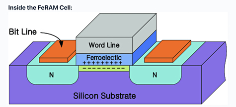
The cell’s binary content is read by the transistor applying a voltage to it and measuring the output. This overwrites the cell’s content meaning it is a destructive read and the cell’s content needs to be rewritten.
The FeRAM market
Up until now FeRAM has been made in small capacity products by suppliers such as Fujitsu, Infineon, SK hynix and Toshiba. Fujitsu has made FeRAM product for more than 20 years. FeRAM is much faster than flash, but has lower density than flash and higher cost, which has restricted its use to applications such as smart electricity meters, programmable logic controllers, airbags, printers, RAID controllers, and RFID tags. Sony’s PlayStation 2 launched in 2000 used 32Kb of Fujitsu FeRAM. Micron’s technology could change this, making FeRAM more generally applicable in the data storage sphere.
FeRAM, as storage-class memory, fits between DRAM and NAND in data access speed and endurance terms. TLC NAND natively has 3,000 to 5,000 write cycle endurance, whereas FeRAM can be rewritten from 100 billion (SK hynix) to 100 trillion (Infineon) times with Micron’s technology supporting 10¹⁵ (10 quadrillion) write cycles. FeRAM’s write cycle time is in the 70 – 120ns area whereas Micron suggests a 300µs write cycle time for NAND.
Micron NVDRAM prospects
Micron’s paper, which is not publicly available, was presented in a Generative AI Focus Session. It discusses a 32Gb die. This is much larger than the Fujitsu and Sk hynix 8Mb products or Infineon’s 16MB and Toshiba’s 128Mb products. However, the gen 1 Optane product had a 128Gb die, four times larger still. The paper abstract says the Micron die has a 2-layer stack, like the gen 1 Optane product. Data is retained for more than 10 years.
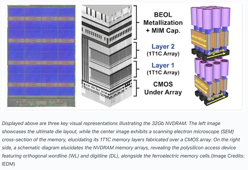
Read and write times are faster than NAND but not as fast as DRAM. Having the technology called NVDRAM (non-volatile dynamic random access memory) is an oxymoron, with NVRAM more appropriate. But NVRAM is a generic term referring to NOR and NAND flash, FeRAM, MRAM and other non-volatile memory technologies, and we guess Micron was looking for a distinctive name.
The paper abstract mentions a “near-term opportunity … to outfit existing, traditional compute architectures with more efficient memory for faster data movement and to accommodate larger models.” This suggests that Micron sees NVDRAM product being used to hold Gen AI datasets and provide faster access to them than SSD storage. Micron’s NVDRAM has an LPDDR5 command protocol interface, which suggests a socket-type interface could be used.
We would envisage that Micron is already exploring commercial possibilities with potential server partners and large scale Gen AI users.
Back in March 2021 when Micron exited the Optane 3D XPoint market it said:”Micron plans to apply the knowledge it has gained from the breakthroughs achieved through its 3D XPoint initiative, as well as related engineering expertise and resources, to new types of memory-centric products that target the memory-storage hierarchy.” FeRAM was probably in its sights then. It also said it “will increase investment in new memory products that leverage the Compute Express Link (CXL) … With immediate effect, Micron will cease development of 3D XPoint and shift resources to focus on accelerating market introduction of CXL-enabled memory products.”
We might well see CXL-accessed NVDRAM product.
B&F has asked Micron for access to the NVRAM paper and for a briefing on the technology.


