


Why is DRAM confined in a 10nm semiconductor process prison when microprocessors and the like are being built using 7nm processes, with 5nm on the horizon? If DRAM could be fabricated with a 7nm process, costs per GB would go down.
However, for the next few years 7nm DRAM is fantasy, due to capacitor and other electrical limitations at the sub-10nm level.
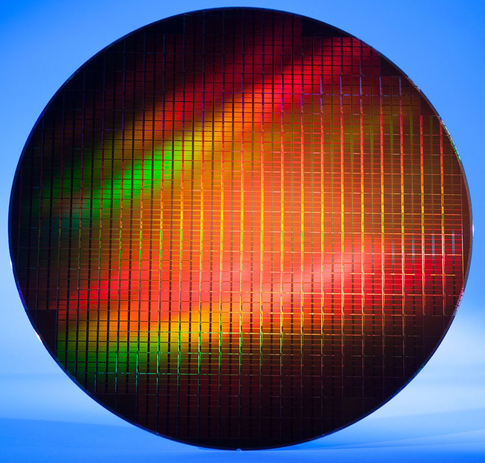
DRAM process shrink progression
DRAM is more expensive and more tricky to manufacture than processor silicon, due to its critical nature. It has to hold data over many logic clock cycles. So it will lag in fabrication processes.
Process size shrinkage is the key to lower DRAM costs. Broadly speaking, the industry standard 300mm semiconductor wafer has a fixed cost. Therefore the more chips you can fit on the wafer the lower the cost per chip.
DRAM process sizes shrank significantly in recent years, until 2016.
- 2008 – 40nm-class – meaning 49nm to 40nm and classed as 4x
- 2010 – 30nm-class – 39nm – 30nm – or 3x
- 2011 – 20nm-class – 29nm – 20nm – or 2x
- 2016 – 10nm-class – 19nm – 10nm – or 1x
Today, vendors are still shipping at the 1xnm node level. There are three sub-levels and the industry refers to them as:
- 1xnm – 19nm – 17nm (Gen1)
- 1ynm – 16nm – 14nm (Gen 2)
- 1znm – 13nm – 11nm (Gen 3)
Next, and in R&D, vendors have three more scaled generations of DRAM on the roadmap, all still at the 1xnm node level. Those are called:
- 1anm (Gen 4)
- 1bnm (Gen 5)
- 1cnm (Gen 6)
Each progression should involve some decrease in DRAM cell size in some dimension to increase density, lower power, etc. The 1a DRAM chips are slated to ship in 2021 or possibly sooner.
DRAM cell sizes are measured using an nF² formula where n is a constant, derived from the cell design, typically between 6 and 8, and F is the feature size of the process technology. Thus, with a 16nm feature size and n=8, then the area is 8 x (16 x 16) = 2,048 square nanometres. Use a 14nm feature size instead and the area is 1,568 square nanometres, 23 per cent less. This is why it is worth shrinking the feature size. You get more GB of DRAM on a wafer that way.
Billions of cells can fit on a single chip, with thousands of cells in a row. Smaller cells can mean billions more in a chip.
Overall we have six 1x-class generations and cannot breach the 10nm process barrier. Why?
Capacitor aspect ratio
The capacitor in a DRAM cell needs to be large enough to store a measurable charge. Shrinking DRAM cell size laterally, by its length and width, decreases the capacitor’s volume, which is, to be blunt, bad: it reduces its effectiveness. This reduction in volume can be compensated for by increasing the capacitor depth or height.
Debra Bell, senior director of DRAM Product engineering at Micron, wrote in an article: “In cell capacitor scaling, the aspect ratio is a challenge.” That’s the ratio between the height and lateral size of the capacitor structure. Make one or both too small and the capacitor cannot do its job effectively.
Increasing the capacitor’s depth has its own problems, as an IBM Zurich research blog stated: “In the long term, this represents a bottleneck – not only due to geometrical constraints, but also because charge accumulation at the top of the ‘well’ makes it more challenging to use the entire storage capacity.”
Another problem is that capacitors leak charge, which is why they have to be refreshed periodically: this is why it is called dynamic random address memory or DRAM, as opposed to static memory, which doesn’t need constant charge refreshing, as data is stored in logic gates but is more expensive. DRAM researchers are looking at getting rid of the capacitor, we hear, by storing the charge in the transistor body using different transistor materials.
Another difficulty is that as cell size decreases and fabricators cram more cells into an array, the relative length of the word and bit lines increases. This affects the time it takes to put a charge in a capacitor and move the charge along the lines.
The net result is that decreasing DRAM cell size beyond the limits met at the 1x nanometer processes is impractical to impossible in the short-term, certainly out to 2025 at earliest. It looks increasingly as if there will have to be some breakthrough in materials to enable us to make the jump into sub-10nm DRAM.
To understand why this is the case let’s take a brief tour of kinds of semiconductor chip manufacturing and DRAM design, where we’ll see the key role played by capacitors.
Under the hood
Random-access memory cells are each made up of tiny circuits, typically involving one transistor that acts as an access gateway, and one capacitor that functions as a charge store. In semiconductor jargon, this design is termed ‘1T1C’ and shown below.
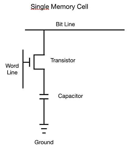
Each circuit is addressable using so-called address strobes. This makes them usable in rows and columns of RAM, called arrays. And each 1T1C circuit in this array is a cell. The cells line up in rows with a bit line connector. Columns of these cells are connected by word lines.
A cell’s address is defined by its location at the intersection of these two orthogonal bit lines and word lines. The address strobes do their work along the word and bit lines as shown in the diagram below.
That’s for memory cells. But logic chips, built out of high-density logic gates, are entirely different. They are super-high density. They are incomparable to 1T1C repetitive building blocks, with relatively large capacitors in them, which is why they can scale down past the 10nm barrier.


 needed to meet archive demand by 2030")