Micron has updated its DRAM roadmap from three to four cell shrink stages, enabling more DRAM capacity per wafer and lowering costs per GB.
The US chipmaker intends to shrink the cell or process node size progressively with the following steps, starting from the no longer mainstream 20nm node process size to the 10nm (19nm-10nm range) node process:
- 1Xnm – (c19-17nm) older DRAM technology process node size
- 1Ynm – (c16-14nm) mainstream DRAM bit production technology today
- 1Znm – (c13-11mn) 15 per cent of Micron DRAM bit production in 3Q20
- 1αnm process node – 1 alpha – volume production in first half of 2021
- 1βnm process node – 1 beta – in early development
- 1ɣnm process node – 1 gamma – early process integration
- 1δnm process node – 1 delta – pathfinding and may need EUV technology
The 1 delta node size is a new entry on Micron’s DRAM roadmap. We do not have indicative process node sizes below 1Znm.
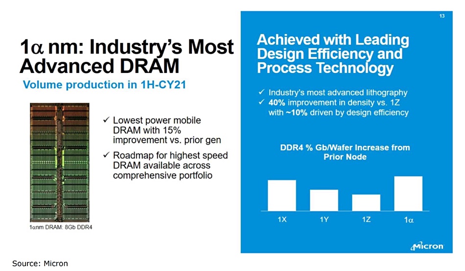
Bit density growth rate slowed with the transitions from 1Xnm to 1Yn and 1Znm, Micron said. However, the company has accelerated the growth rate with a 40 per cent increase from 1Znm to the 1αnm process node size.
Wells Fargo analyst Aaron Rakers informs subscribers Micron has a strong position in 1Znm DRAM production. Citing the research firm DRAMeXchange, he estimates Micron’s 1Znm output at 15 per cent of its DRAM bit production in 3Q20 versus Samsung and SK hynix at six per cent and zero.
Other things being equal, 1Znm DRAM costs less to manufacture than the preceding 1Ynm node.
In Violet
Micron uses Deep Ultra Violet (DUV) multi-patterning lithography to lay out DRAM cell die details on a wafer. As the process node size in shrinks below the 10nm cell size level, the wavelength of the light beam becomes a constraint.
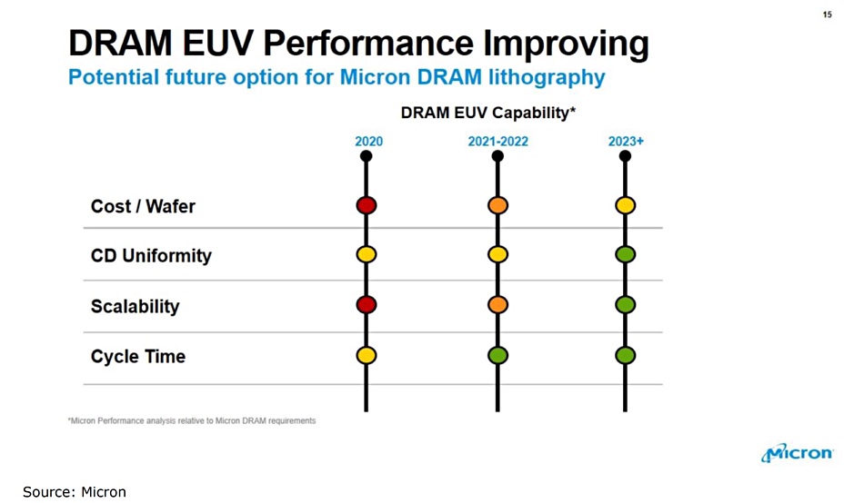
ASML, the dominant supplier of lithography machines for the chip industry, has developed EUV (Extreme Ultra Violet) scanners which emit smaller wavelength light. This technology etches narrower lines on the wafer and so enable smaller process sizes – i.e. more DRAM dies on the wafer, and consequently higher capacity per wafer and lower cost per GB. But the capital outlay is significant – currently ASML makes only 30 EUV lithography machines a year – they weigh 180 tons and cost $120m each.
Samsung use EUV in 1Znm process nodes and SK hynix plans to use EUV technology for volume production of 1αnm DRAM and1βnm DRAM. Micron thinks EUV will not be cost-competitive until 2023 or later, meaning the 1δnm process node.