


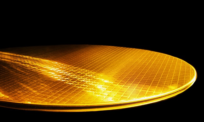
Micron is starting production shipments of its 232-layer NAND chips, making it the first flash chip maker to cross the 200+ layer 3D NAND barrier.
Scott DeBoer, MIcron’s EVP for technology and products, said: “Micron’s 232-layer NAND is a watershed moment for storage innovation as first proof of the capability to scale 3D NAND to more than 200 layers in production.”
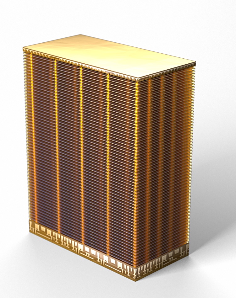
Chip details include:
- 2.4GB/sec IO speed;
- 50 percent more than Micron’s 176-layer product’s 1.6GB/sec
- 100 percent more write bandwidth than 176-layer chip
- Up to 77 percent higher read bandwidth than 176-layer chip
- 6 planes (access lanes), the most planes per die of any TLC flash with independent read capacity per lane
- TLC format (3bits/cell) with highest TLC density per square millimeter ever produced (at 14.6 Gbit/mm squared
- NV-LPDDR4 low-voltage interface support, meaning per-bit transfer savings of up to 30 percent plus compared to the LPDDR4 interface
- New 11.5mm x 13.5mm package, 28 percent smaller than previous Micron NAND chip generations
The chip’s endurance has yet to be revealed.
Micron claims that the chip’s areal density is between 35 and 100 percent more than competing TLC products in the market. Its small size means it can be used in small smart devices needing more flash, such as cameras, video recorders, mobile phones and gaming consoles.
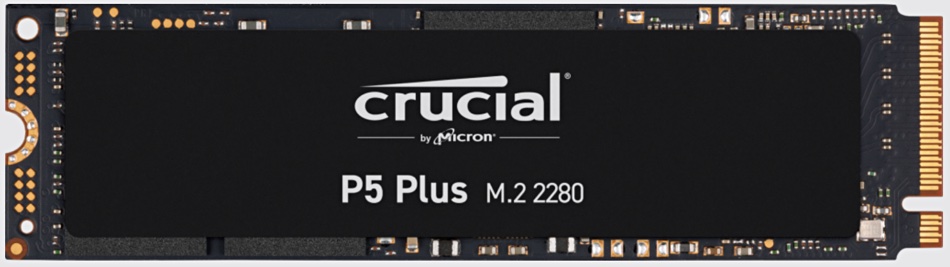
Micron’s 232-layer NAND is now shipping to customers in component form and through its Crucial SSD consumer product line.
Currently, Crucial ships 176-layer TLC M.2 (gumstick card) 2280 format NVMe SSDs such as the P2, P3, P3 Plus and P5 Plus gaming SSD. The latter uses the PCIe gen 4 bus and has 500GB, 1TB and 2TB capacities, and up to 6.6GB/sec read and 5GB/sec write speeds. It provides up to 720,000 random read IOPS and 700,000 random write IOPS.
A 232-layer version of the P5 Plus would nominally deliver up to 10GB/sec write bandwidth and 11.68GB/sec read bandwidth – mouth-watering speeds. The read and write IOPS numbers should also increase.
Samsung said it had working 200-layer 3D NAND technology a year ago, and may introduce a 200+ layer product by the end of the year. It could possibly be 224 or even 256 layers using two component dies with a string-stacking approach.
Yesterday we reported YMTC has 232-layer technology in its roadmap.


