


Micron has 232-layer 3D NAND in development and a roadmap out to 500-plus layers.
3D NAND is manufactured by layering groups of cells atop each other in a vertical stack. The more layers there are in a flash die, the higher the capacity. All the manufacturers are currently building 100-plus layer chips with higher layer counts in prospect.
Yesterday Western Digital revealed it was building 162-layer NAND with a 200+ layer die coming.
Micron revealed its NAND and DRAM roadmap details at an Investor Day event on May 12. It is manufacturing 176-layer flash chips in volume, its fifth 3D NAND generation, and intends to ramp up manufacturing of sixth-generation 232-layer flash by the end of calendar 2022.
A slide provided staged layer count increases out to the 500-plus level, but with no timescale:
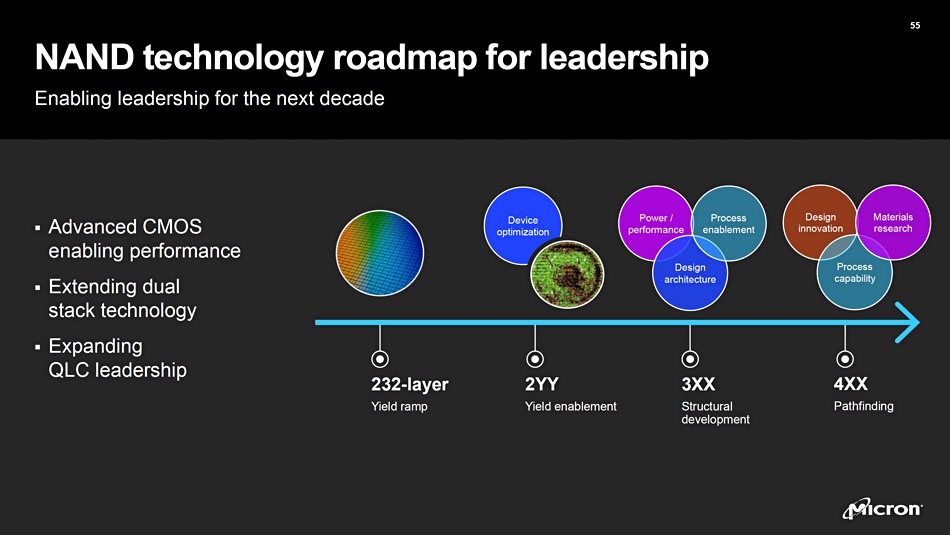
The dual stack technology refers to stacking two 3D NAND dies one above the other, so-called “string stacking.” This overcomes semiconductor manufacturing difficulties such as etching connection holes through the layers as the number of layers increases. The sides of such holes can become distorted as hole depth deepens and prevent the NAND cells from operating properly.
Micron said it was focusing on QLC (4bits/cell) NAND and didn’t mention increasing the cell bit count to 5 with PLC (penta-level cell), which Western Digital is investigating and Soldigm developing. We think this is because Micron is being cautious and not that it has rejected PLC NAND as infeasible.
Here is a table comparing the NAND manufacturers’ 3D NAND layering status, history and plans:
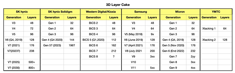
WD would say there is no inherent superiority in having a slightly higher layer count – 238 (SK hynix), 232 vs 212, for example – because it is shrinking its cell size laterally, in width and length, as well as increasing the die height by adding layers. The combination of the two techniques means that it can increase die density to the same or greater degree as its competitors and have fewer layers.
There is an implied advantage here as building a layer means making a group pf processing steps and, other things being equal, making 232 processing groups takes longer than making 212. But so many other things come into play, such as wafer manufacturing yield, that the end result; manufacturing cost, chip density price, endurance and performance, is not based only on the number of manufacturing steps.
Micron claims that its 232-layer technology represents the world’s most advanced NAND:
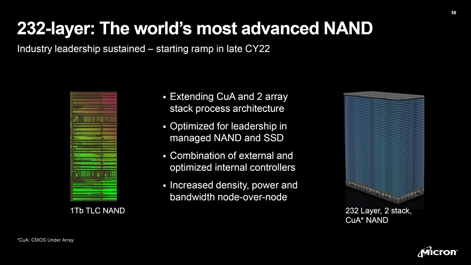
This slide showed a 1Tb (128TB) TLC die. Micron did not mention zoned SSDs in its presentation but it did talk about external controllers, implying NAND/SSD controllers operating in the host system, which is necessary with zoned SSDs. We might expect to see SSDs using the 232-layer NAND to ship in late 2023.
The Investor Day did not cover storage-class memory, such as 3D XPoint, which it used to manufacture for Intel. But it did talk about CXL (Computer eXpress Link) and a slide showed something called emerging memory technology at the end of a CXL link:
Another talked about “New Memory architecture” and “CXL roadmap focus on customer co-invention,” whatever that might mean. It could imply possible customer-specific, CXL-linked memory devices. We think emerging memory and new memory architecture could apply to storage-class memory and/or to 3D DRAM.
NAND roadmaps from Solidigm, Western Digital, and Micron testify to the technology health and vitality of the NAND and SSD markets, meaning we can look forward to growing flash data storage capacity and increased application speed.


