


Compared to NAND flash, Intel’s Optane DIMM product is low on capacity and high on price. Increasing its capacity should lower the cost/GB and so help address both issues. How might this be done?
Optane DC Persistent Memory is Intel and Micron’s 3D XPoint (3DXP) in a DIMM form factor with 128GB, 256GB and 512GB capacities. This is the first generation of 3DXP technology and features two stacked layers of single bit cells built with a 20nm process technology and a 128Gb die.
The cell size is 0.00176 µm2; roughly half the size of a DRAM cell.
Capacity increases in NAND technology have come from reducing cell size through smaller process geometries – traditional lithographic pitch scaling – and then implementing multiple layers and increasing the number of bits per cell. The semiconductor industry is currently transitioning from 64 to 96 layers, for example. TLC NAND has 3 bits/cell and the newly introduced QLC has 4.
3D layering used larger process sizes than the 14 – 15nm seen in 2D or planar NAND, moving to 40nm or so, and offsets the reduced number of cells per layer with a big increase in layer count.
So a quick comparison is that 3DXP is a 2-layer, single bit/cell design built with a 20nm process while current NAND is a 64-layer, 3bits/cell design made from a 40nm process.
This suggests three possibilities for 3DXP capacity increases: shrinking the process size, adding more layers, and increasing the number of bits per cell.
My supposition is that Micron will introduce a gen 2 3DXP product when it unveils its own 3DXP products towards the end of this year. It is already making gen 1 3DXP chips in the IMFT foundry and so has no technological need to wait until the end of 2019 to introduce its own branded 3DXP product. Ergo it is tweaking the technology.
How practical are the three capacity increase ideas identified here?
Process size shrink
Micron mentions process size shrink as a possibility but supplies no example numbers.
We could speculate that gen 2 3DXP could use a 15nm process, representing a 25 per cent reduction in size, with a consequent increase in the number of XPoint dice you could obtain from a wafer.
But we don’t know the yield of XPoint chips from a wafer and so can’t estimate the effect of this.
Layering
Doubling the layer count from 2 to 4 would double the capacity of the 3DXP die from 128Gb to 256Gb. Quadrupling it to 8 layers would get us a 512Gb die and moving to 16 layers would produce a 1Tb die. That represents an eightfold increase in capacity.
Micron and Intel will have learnt a lot about layering from 3D NAND and it seems reasonable to assume that increasing 3DXP’s layer count is feasible and could deliver significant capacity increases.
Multi-bit cells
The recording medium in 3DXP is Phase-Change memory and IBM has demonstrated TLC Phase-Change Memory. A 3-bit cell would increase 3DXP capacity threefold, from a 128Gb die to a 384Gb die. That’s useful but less dramatic than a layer count increase.
Development priority
If the development priority is to increase capacity then bulking up the layer count seems to deliver most bangs for the buck. Tripling the cell bit count would deliver a threefold capacity increase. Reducing the cell size would produce an increase of two to three times.
I think it makes more sense to develop one method rather than two or three, as stacking layers on a known process geometry would be more practical than stacking layers on an untried and new, smaller process geometry.
These are my initial thoughts about 3DXP technology. What does the semiconductor industry think? Umm… Micron “has decided not to comment on this occasion.” And Intel has yet to come back to us. Let’s see what the analysts have to say.
Jim Handy
Jim Handy, a semiconductor analyst at Objective Analysis, sees 3DXP’s market situation: “as a competitor to DRAM, not NAND flash. This lowers the bar a considerable amount.”
“Although 3D XPoint SHOULD be cheaper than DRAM based on the cell size (as you say) or, more simply, the number of bits per die area, it has failed to achieve that goal. his is because its production volume is too low. The “economies of scale” are in the way.
“NAND flash had the same issue, although it wasn’t originally vying to compete against DRAM. You can get twice as many SLC NAND bits on a certain size die as you can DRAM bits, when they are both made using the same process geometry. This has always been true. Yet, NAND flash GB were more costly than DRAM until 2004, the year when NAND flash wafer production first came within an order of magnitude of DRAM wafers. ”
Handy concludes: “NAND had to reach near-DRAM volumes to match DRAM costs. 3D XPoint must meet the same requirement to match DRAM costs. Yet, there’s no real market for 3D XPoint unless it is sold for sub-DRAM prices.”
How do you square this circle?
According to Handy, “Micron knows exactly what 3D XPoint costs to produce, and the company is also fully aware of what it sells for. Guess why their 3D XPoint products have been pushed out? Guess why Intel’s Storage Devices Group has been losing money while other NAND flash makers have been reaping handsome profits?
He supplies a chart to illustrate this point:
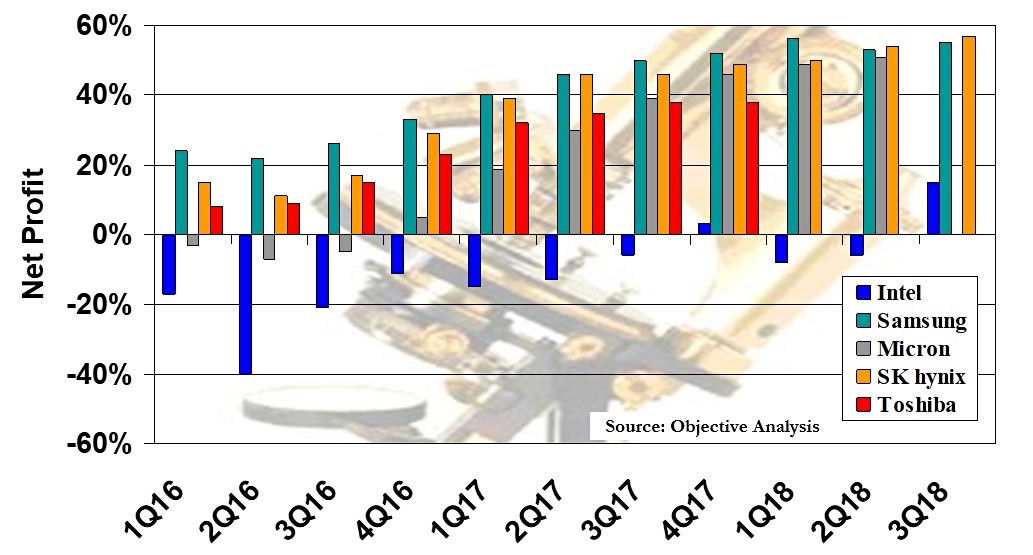
“Whenever 3D XPoint volume gets sufficiently high then all this will straighten out, and Intel will profit from a product that sells for maybe half as much as DRAM but costs less than that to produce. It’s not there yet.
“Unfortunately for Intel, the DRAM market has started its 2019 price collapse (which we have been anticipating since late 2015) and this will require 3D XPoint prices to keep pace, worsening Intel’s losses.”
Handy’s view of 3DXP layering
Handy says 3DXP Layering is more difficult than NAND Layering; “There’s a BIG difference between 3D XPoint layers and NAND layers. With NAND you put down scads of layers (32, or 48, or even 64) and then do a single lithographic step, and then it’s usually at a relaxed process like 40nm.
“With 3D XPoint the device needs to be patterned with a more advanced (and costly) lithography, which is 20nm today, for every single layer of bits. This is because you have to run conductors north-south on the first layer, then east-west on the next layer.
“This not only adds phenomenally more cost than you have with a 3D NAND process, but it also complicates processing to the point where some process experts doubt that it will ever be economical to produce any kind of crosspoint chips with more than 4 bit layers. (See this 4DS presentation from the 2016 Flash Memory Summit.)
That, if true, is a major difficulty.
Handy on adding 3DXP cell bits
“MLC and TLC are unlikely to be used for 3D XPoint because multibit technology is really slow. Optane needs to support near-DRAM speeds.”
That’s true for Optane DIMMs but the SSD situation could differ;
“Perhaps MLC/TLC would be good for cost reductions on Optane SSDs, but the market acceptance for these has been very low so far, and I don’t expect for that to change. The NVME interface hides most of 3D XPoint’s speed advantage. I documented that in a 2016 blog post.
His overall conclusion is bleak: “In a nutshell, I don’t expect for 3D XPoint prices to ever approach NAND’s prices, and it can’t take advantage of any of the advancements in 3D NAND processing. It should, though, eventually be a cost-effective competitor to DRAM, but it’s unclear how long it will take to get there.
“Over the long term, if 3D XPoint succeeds, all systems will ship with very small DRAMs and a very large compliment of 3D XPoint Memory. Over the next 12-18 months, though, the big challenge will be to attain costs that allow a profit while DRAM prices continue to fall.”
Here’s a second chart Handy supplied, to show DRAM spot prices being a leading indicator of DRAM contract prices:
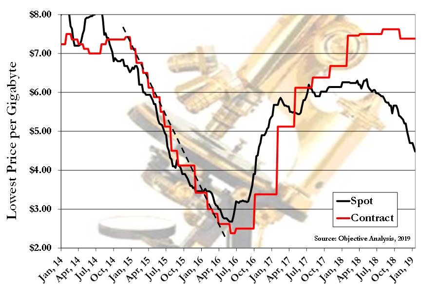
It looks as if a tremendous price drip is coming for DRAM contract prices.
Howard Marks
The founder and chief scientist at DeepStorage Net gave us a typically pithy comment: “I’m hopeful about XPoint 2.0. [having] 8 layers so the remains of IMFT can sell Xpoint at 2X flash prices not 5X … [That] would be nice.”
Rob Peglar
Rob Peglar, President of Advanced Computation and Storage LLC, said that prospects for increasing the capacity of 3DXP DIMMs centre on increasing die capacity: “This is really about the density of each 3DXP die more than the # of die they can squeeze onto a DIMM form factor (which is standardised by JEDEC.)”
He clarified our thinking on shrinking 3DXP process size: “You can be certain that Micron won’t divulge process sizes, yields, or any other fabrication-related detail. Par for the course with the semiconductor vendors 🙂
“Also, if you want to speculate, know that going from 20nm to 15nm is a huge decrease; it’s not 25 per cent, it’s nearly 50 per cent, because it’s the area (2D) of the cell, not just the width (1D), that is reduced. For comparison, NAND went from 20nm to 18nm to 16nm, and it took quite a while to do that. 20nm to 15nm is nearly impossible.”
Peglar also thinks adding bits to a 3DXP cell is problematic:
“Multi-bit is very difficult in crosspoint-style interconnections, as opposed to non-crosspoint-style interconnects. While not outside the realm of possibility, it’s a (very) long shot.”
The net conclusion from this is that increasing the layer count looks the most practical route to increasing 3DXP density.
Conclusion
Increasing its layer count appears to be the only viable short-term way of increasing XPoint die (and hence DIMM) capacity. This is harder to do than adding layers in 3D NAND manufacturing. Unless 3DXP’s process size can be reduced this may drastically limit 3D XP’s density increase possibilities.


