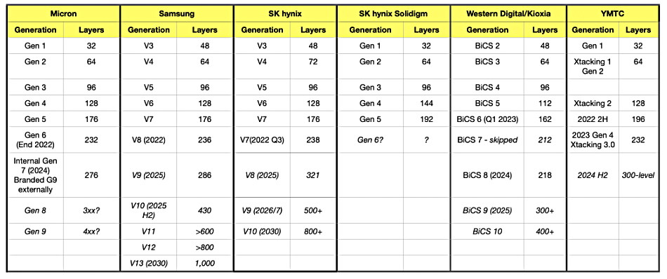
Micron has announced the 2650 client SSD, its first product built from 276-layer 3D NAND, 18 months since it launched the 2550 client SSD using 232-layer NAND.
The 276 layers are a record for Micron, which presents this as its 9th generation 3D flash. The 2650 is a TLC (3bits/cell) product and uses a PCIe gen 4 interface, like the 2550. It has capacity points ranging from 256 GB to 1 TB and Micron claims it offers best-in-class performance.

The Gen 9 NAND is claimed to have the industry’s fastest IO speed at 3.6 GBps, beating competitive products from SK hynix, Solidigm, Kioxia, Western Digital, and Samsung with up to 99 percent faster read and 88 percent better write bandwidth. Micron also claims that its Gen 9 NAND is up to 73 percent denser and 28 percent smaller in board size than their products.

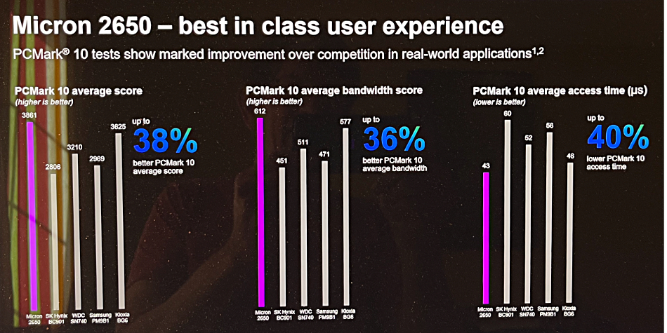
The 2650 comes in the M.2 gumstick format, with 2230, 2242, and 2280 sizes. Micron hasn’t disclosed its IOPS and bandwidth numbers, but has revealed PCMark 10 benchmark results versus products from SK hynix (BC901), Kioxia (BG6), Western Digital (SN740), and Samsung (PM9B1):

It claims up to 38 percent better average score, 36 percent average bandwidth, and 40 percent faster access time.
This 2650 contrasts with Micron’s 9550 datacenter SSD, which was launched a few days ago. It uses Micron’s Gen 8 232-layer NAND and, with its PCIe gen 5 interface, has very high performance numbers.
We asked Micron some questions about the new 276-layer NAND.
Blocks & Files: What was the thinking behind such a relatively modest layer count increase, from 232 to 276 layers?
Micron: The optimal customer design points, not layer count, drove our decisions for Micron G9 NAND. Primary among these was the need to create a 1 Tb die that fits in an 11.5 x 13.5 mm BGA package while delivering 3.6 GBps. This focus helped us deliver breakthroughs in performance and package size along with 44 percent higher bit density compared to our prior generation. These advancements collectively contribute to a superior NAND solution that addresses the needs of our customers.
Blocks & Files: Is the die single or multi-stacked (two or three stacks)?
Micron: Our G9 TLC NAND uses a single die and class-leading six-plane architecture, allowing us to deliver the necessary performance and requisite costs to meet our customers’ needs.
Blocks & Files: Has it been scaled down in physical size from the 232-layer NAND product, and, if so, how?
Micron: We maintain our best-in-class 11.5 x 13.5 mm BGA package size, which uses up to 28 percent less board area compared to the larger 12 x 18 mm package still being used by most of our competitors. This enables optimal PCB layout, signal routing, and thermal performance, which is especially important for newer SSD form factors, like E1.S and E3.S.
Blocks & Files: Does Micron anticipate producing a QLC version of the G9 276L die?
Micron: While we generally do not comment on future announcements, we maintain our commitment to QLC NAND innovation in the industry.
According to Forward Insights, Micron’s mix of QLC NAND bit shipments in CQ1-24 was the highest among major NAND providers.


