Israeli startup RAAAM Memory Technologies has announced $4 million in seed funding to develop a System-on-Chip (SoC) SRAM replacement.
Robert Giterman, RAAAM co-founder and CEO, said in a statement: “RAAAM’s Gain-Cell Random Access Memory (GCRAM) technology is a unique on-chip memory solution that only requires three transistors to store a bit of data, as opposed to 6-8 transistors needed for the existing SRAM-based highest-density memory technology. The GCRAM solution reduces area by half and power consumption by a factor of five and can be manufactured cost efficiently using the standard CMOS process.”

RAAAM says GCRAM is fully compatible with standard CMOS and can be used as a drop-in SRAM replacement in any SoC, allowing for lower fabrication costs through reduced die size or enhanced system performance by increasing memory capacity within the same die size.
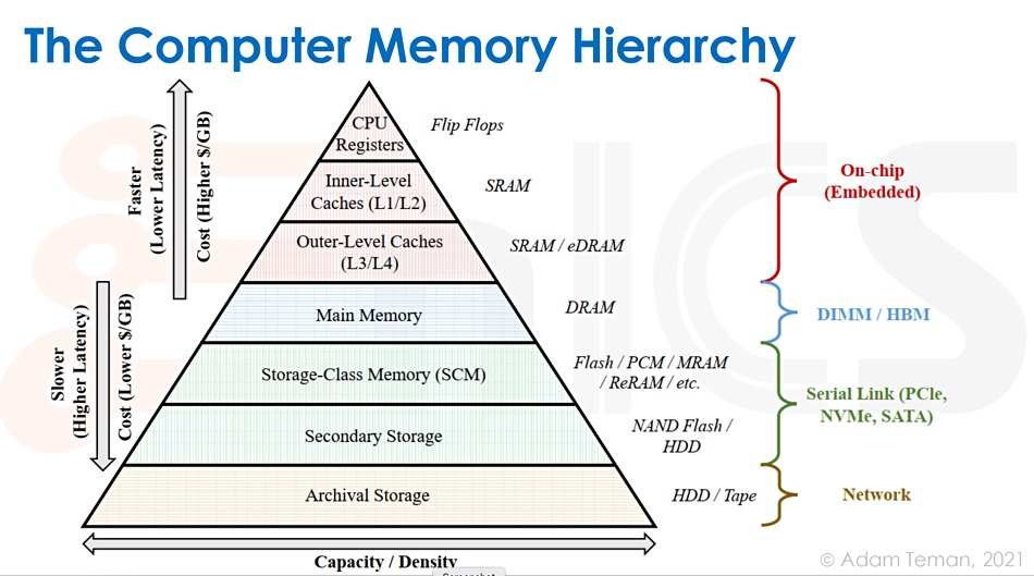
The firm says that SoCs are devoting increasing amounts of their on-chip area to embedded memory, typically SRAM. As our glossary states, SRAM uses a flip-flop circuit with two stable states to store a binary bit value. The circuit needs four transistors to store a bit and two to control access to the cell. In contrast, DRAM needs one transistor and one capacitor to store a bit, making its cells smaller than SRAM cells. RAAAM says the size of SoC embedded memory is increasing, reaching up to 75 percent of the total SoC real estate in some applications like artificial intelligence and machine learning. This will limit SoC development and applicability.
It was founded in 2021 by four PhDs from Bar-Ilan University and the Swiss Federal Institute of Technology Lausanne (EPFL) that specialize in Very Large-Scale Integration (VLSI) design. These are Giterman plus Andreas Burg, Associate Professor, Head of the Telecommunications Circuits Lab at EPFL, Alexander Fish, Professor at Bar-Ilan University and Advisor, and Adam (Adi) Teman, Associate Professor at Bar-Ilan University and Scientific Advisor.

Seed round investors include Serpentine Ventures, J-Ventures, HackCapital, Silicon Catalyst Angels, Claves Investments, and a large multinational semiconductor company as a strategic investor.
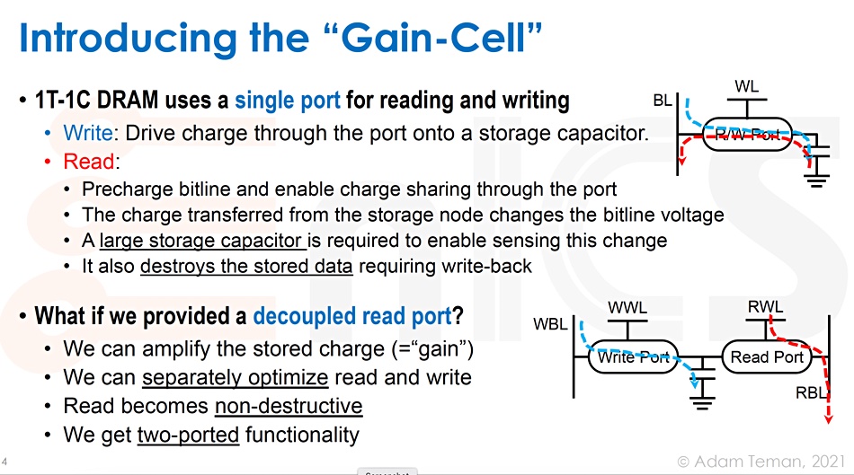
A downloadable GCRAM presentation, created by Adam Teman, explains how the technology uses separate read and write ports, in contrast to DRAM’s combined read/write port per cell. This enables it to amplify the cell’s stored charge and separately optimize the read and write processes while retaining SRAM-like performance.


