


Micron has launched both a fingernail-sized flash storage device for smartphones and a large high bandwidth memory chip for Nvidia GPUs.
Flash and DRAM foundry operator Micron builds and sells SSDs. The flash chip is an enhanced version of a UFS 4.0 format device, 9 x 13 mm in size, with up to 1 TB in capacity using Micron’s 232-layer 3D NAND technology. It delivers twice the performance of UFS 3.1 specification devices, pumping out up to 4,300 MBps sequential reads and 4,000 MBps sequential writes. Smartphone apps can be launched in less time and run faster, and the device can be used in automotive applications as well.
Micron’s Mobile Business Unit GM and corporate VP, Mark Montierth, said in a statement: “Micron’s latest UFS 4.0 solution enables world-class storage performance and reduced power in the world’s smallest UFS package. Supercharged with breakthrough firmware advancements to keep smartphones running like new, Micron UFS 4.0 raises the bar for mobile storage with enhanced performance, flexibility and scalability to accelerate the rollout of generative AI-capable smartphones.”
The company claims large language models in generative AI apps can be loaded 40 percent faster than Micron’s prior 176-layer UFS 3.1 product, resulting in a smoother experience when initializing conversations with chatbots. This prior product was physically larger, measuring 11 x 13 mm, and needed more electricity. The new one is said to be 25 percent more power-efficient.
The chip’s firmware has three new features:
- High-Performance Mode (HPM): This optimizes performance by prioritizing critical tasks over background ones during intensive smartphone use, with an over 25 percent speed improvement when launching multiple apps over the UFS 3.1 product due to twice-as-fast storage access during heavy usage.
- One Button Refresh (OBR): Automatically cleaning and optimizing data so smartphones can continue operating in a like-new state.
- Zoned UFS (ZUFS): The host can specify different zones where data can be stored, improving the usefulness of the device over time. This ZUFS approach reduces write amplification to extend the flash lifespan, keeping devices feeling like new for longer.
Micron is now shipping samples of its upgraded UFS 4.0 drive in capacities of 256 GB, 512 GB, and 1 TB. It announced that both HONOR and Samsung are using its LPDDR5X memory and UFS 4.0 mobile flash storage in their latest AI-driven smartphones, the HONOR Magic6 Pro and the Samsung Galaxy S24 series.
Nvidia HBM3e
Micron is building 24 GB HBM3e (High Bandwidth Memory gen 3 extended), with 8 x 3 GB stacked DRAM dies, for use by Nvidia in its H200 Tensor Core GPUs, due to ship next quarter. The H200 is a high-end GPU, a refresh of the existing Hopper architecture H100 intended for AI processing work. It should come with up to 141 GB of HBM3e memory and 4.8 TBps of bandwidth, meaning up to six Micron HBM3e chips per H200.
We’re told that the pin speed of Micron’s HBM3e device is >9.2 Gbps and its overall speed is >1.2TBps. Micron claims it has around 30 percent lower power consumption than unidentified competitive offerings.
EVP and Micron Chief Business Officer Sumit Sadana said: “Micron is delivering a trifecta with this HBM3e milestone: time-to-market leadership, best-in-class industry performance, and a differentiated power efficiency profile.
“AI workloads are heavily reliant on memory bandwidth and capacity, and Micron is very well-positioned to support the significant AI growth ahead through our industry-leading HBM3e and HBM4 roadmap, as well as our full portfolio of DRAM and NAND solutions for AI applications.” Getting Nvidia as a customer is a good win for Micron, and steals a march on rivals Samsung and SK hynix. In its last earnings call, back in December, Micron CEO Sanjay Mehrotra said: “We are on track to begin our HBM3e volume production ramp in early calendar 2024 and to generate several hundred millions of dollars of HBM revenue in fiscal 2024. We expect continued HBM revenue growth in 2025.” The Nvidia deal must have been visible to Mehrotra then.
Micron will be sampling a larger HBM3e product in March, with a 12-high stack of DRAM chips yielding 36 GB in capacity, and >1.2 TBps performance again.
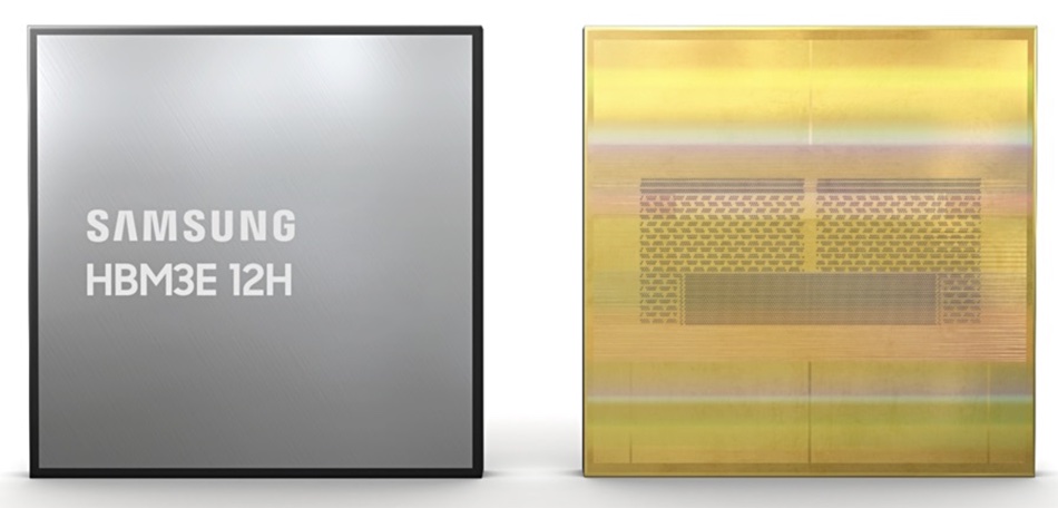
But Samsung has announced its own 12-high, 36 GB HBM3e device, with up to 1.28 TBps bandwidth. It builds the 12-layer device using a thermal compression non-conductive film (TC NCF) to squeeze it down to the same height as a 8-layer device. This technique mitigates chip die warping that can come with a thinner die. Sammy says it’s lowered the thickness of its NCF material and achieved the industry’s smallest gap between chips at seven micrometers (µm), and eliminating voids between layers. This results in enhanced vertical density by over 20 percent compared to its HBM3 8-layer product.
Yongcheol Bae, EVP of Memory Product Planning at Samsung Electronics, said: “This new memory solution forms part of our drive toward developing core technologies for high-stack HBM and providing technological leadership for the high-capacity HBM market in the AI era.”
Expect more Micron HBM3e details at the Nvidia GTC event on March 18.


