


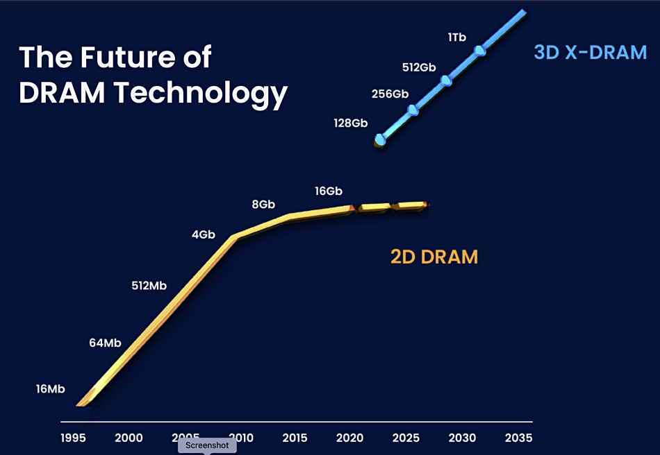
Startup NEO Semiconductor suggests its 3D X-DRAM technology could produce a 128Gbit DRAM chip with 230 layers – eight times more than current DRAM density.
Update. Andy Hsu comments on floating body technology added, 5 May 2023.
NEO is focused on semiconductor memory and has developed X-NAND technology, NAND dies with multiple parallel planes to speed data access – 1,600MBps sequential write bandwidth in gen 1 and 3,200MBps in gen 2. It says there is an industry-wide effort under way to bring 3D cells to DRAM and NEO now has 3D DRAM technology. Like 3D NAND, it could drive up DRAM density significantly.
Andy Hsu, co-founder and CEO, bullishly said: “3D X-DRAM will be the absolute future growth driver for the semiconductor industry.” Hsu was with an unnamed semiconductor startup for 16 years after graduating with a Masters from the Rensselaer Polytechnic Institute in 1995. He founded NEO Semiconductor in August 2012 and has 12 patents to his name. NEO itself has 23 patents.
He added: “Today I can say with confidence that NEO is becoming a clear leader in the 3D DRAM market. Our invention, compared to the other solutions in the market today, is very simple and less expensive to manufacture and scale. The industry can expect to achieve 8X density and capacity improvements per decade with our 3D X-DRAM.”
NEO says 3D X-DRAM is necessary to address the increase in demand for high-performance and high-capacity memory semiconductors driven by the next wave of AI applications such as ChatGPT.
A graphic shows the 3D X-DRAM concept:
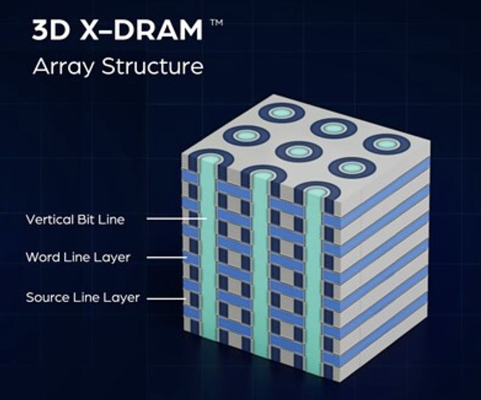
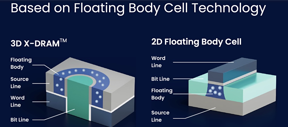
The concept has a 3D NAND-like DRAM cell array structure based on capacitor-less floating body cell (FBC) technology. This FBC technology stores data as electric charges using one transistor and zero capacitors. NEO says it can be manufactured using current 3D NAND-like processes and only needs one mask to define the bit line holes and form the cell structure inside the holes. This provides a high-speed, high-density, low-cost, and high-yield fabrication solution, which is a significant claim.
Jay Kramer, president of Network Storage Advisors, a marketing consulting service, said: “Evolving from 2D to 3D architectures has introduced compelling and extremely valuable benefits to NAND flash, so achieving a similar evolution for DRAM is highly desirable industry-wide. NEO Semiconductor’s innovative 3D X-DRAM allows the memory industry to leverage current technologies, nodes and processes for enhancing DRAM products with NAND-like 3D architectures.”
NEO suggests 3D X-DRAM could scale past a 1Tb chip in the 2030-2035 period:
We understand NEO will be looking to license its technology to DRAM fabrication companies such as Micron, Samsung, and SK hynix. NAND fabbers like Kioxia and Western Digital could also be licensing possibilities.
Relevant 3D X-DRAM patent applications were published with the United States Patent Application on April 6, we’re told. US patent 20230106561 by Fu Chang Hsu, 30 Sep 2022, is entitled 3D Memory Cells and Array Architectures. Its summary states: “a novel 3D array structure using floating-body cells to implement DRAM is disclosed. The array structure is formed using a deep trench process similar to 3D NAND flash memory. Therefore, ultra-high-density DRAM can be realized.”
Bootnote
Neo Semiconductor has disclosed no funding information and LInkedIn shows just two employees; co-founders Andy “Fu Chang” Hsu and VP Engineering Ray Tsay. Both worked at a semiconductor startup; no name revealed but possible Aplus Flash Technology, involved in NOR flash, EEPROM and NVSRAM for 16 years and 11 years respectively before founding Neo Semiconductor. Andy Hsu is said to hold more than 100 patents. LinkedIn lists a third Neo Semiconductor employee; Hong Cui, but lists him or her as an engineer at Nero Semiconductor.
Update
Andy Hsu commented on a Linkedin post saying: “The early 2D floating body cell from 2000 – 2010 had some issues, especially when the cell size shrunk, the floating body became smaller. Unlike DRAM that can make the capacitor taller to keep the same capacitor size, 2D floating body cell has no way to increase the capacitor size. Recently, many research has been done by using new mechanisms such as heterostructure or polysilicon grain boundaries for storage and showed excellent data retention. Plus, 3D floating body cells’ size (diameter >100 nm) is much larger than 2D floating body cells, that provides enough capacitance for charge storage. The announced cell structure is just the basic form. The real structure may contain other features. We will disclose more details in FMS 2023.”


