Kioxia, formerly known as Toshiba Memory, has devised a way to make 3D NAND cells smaller and so reduce the layer count needed to reach a capacity level.
A floating gate is the part of a Kioxia NAND cell that holds the charge designating a binary one or zero. An electric current senses if the charge state flows through the gate or not, indicating the binary value. The structure is called a floating gate because the charge value and electricity flow changes.
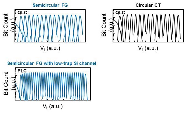
In Kioxia’s 3D NAND technology, known as BiCS (bit column stacked), the floating gate has a circular form and the cells are built in layers with the layer count and cell bit count increasing to make higher capacity NAND chips. 64-layer 3D NAND is being succeeded by 96-layers and TLC (3bits/cell) is progressing to QLC (4bits/cell). Penta-level cell technology (PLC or 5bits/cell) is on the horizon.
However, QLC flash needs to support 32 different voltage levels per cell instead of QLC’s 16, and progressing beyond 96 layers to 100-plus is creating manufacturing difficulties. It is harder to etch holes precisely in the structures, craft cells with a uniform size and get good yields from NAND wafers. These problems are worse still with PLC NAND.

Kioxia’s engineers have lowered the time to write data to cells by splitting the circular gate into two semicircular halves. This design results in lower electron leakage, and the cells can be made smaller too. In turn, more cells will fit on a wafer and fewer layers are needed to reach a capacity level. Kioxia calls this ‘Twin BiCS’ and says the technology makes PLC NAND manufacturing more feasible.
If this technology enables a significantly lower number of layers and the use of PLC NAND at any capacity point, such as 1TB, rival NAND manufacturers will have to develop comparable technology to keep their costs and prices in line with Kioxia.
Kioxia announced Twin BiCs at the IEEE International Electron Devices Meeting (IEDM) held in San Francisco, CA on December 11.


