


The Flash Memory Summit lived up to its major flash technology revelation status with news of penta-level cell flash.
Toshiba Memory and Western Digital operate a NAND fabrication joint-venture. In presentations at FMS in Santa Clara yesterday, the companies talked about PLC NAND in the context of responding to general data growth by increasing flash storage capacity.
Penta-level cell or PLC flash has five bit levels per cell. The continues the progression from SLC (1 bit/cell), MLC (2 bits/cell), TLC (3 bits/cell) and today’s developing QLC (4 bits/cell).
PLC details
The number of bits stored in a cell depends upon the number of voltage levels, and thus the binary values it can have:
- SLC = 0 or 1 – meaning two states and one threshold voltage,
- MLC = 00, 10, 01, or 11 – four states and so three threshold voltages,
- TLC = 000, 001, 010, 011, 100, 101, 110, 111 – eight states and thus seven threshold voltages,
- QLC = 0000, 0001, 0010, 0011, 0100, 0101, 0110, 0111, 1000, 1001, 1010, 1011, 1100, 1101, 1110, 1111 – 16 states and so 15 threshold voltages,
- PLC = 00000, 00001, 00010, 00011, 00100, 00101, 00110, 00111, 01000, 01001, 01010, 01011, 01100, 01101, 01110, 01111, 10000, 10001, 10010, 10011, 10100, 10101, 10110, 10111, 11000, 11001, 11010, 11011, 11100, 11101, 11110, 11111 – 32 states and so 31 threshold voltages.
A PLC cell has 25 per cent more capacity than a QLC cell. Therefore a 256GB QLC SSD will become a 320GB PLC SSD when organised into penta-level cells. The flash manufacturer gets that extra capacity from a flash wafer without much increase in manufacturing expense and the cost per bit goes down.
This short life
However, the endurance (read/write cycles) and speed of PLC NAND will be less than that of QLC flash, which is less than that of TLC flash and so on. Endurance also reduce as the cell process size decreases. Simply put, the number of electrons available in a cell to indicate a voltage level diminishes as the process size shrinks.
Here is a table of representative raw endurance numbers for flash with different cell levels and different process sizes:
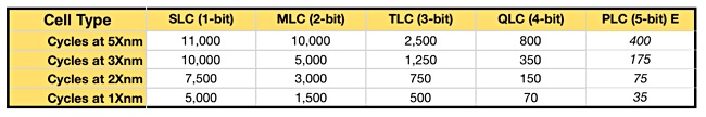
These are example numbers, dating from before the 3D NAND era, and different manufacturer’s NAND products will vary. We have estimated the PLC column numbers as none have been released by the manufacturers.
Charting this provides an instant view of how short-lived the working life of PLC flash can be in terms of write cycles;
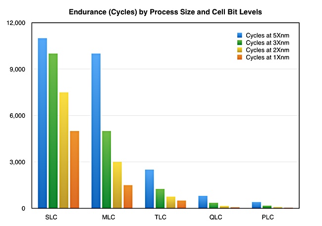
The short cycle life of PLC flash will limit its applicability.
SSD suppliers can mitigate this short life by reducing the number of writes needed during storage operations and by supplying extra cells to replace worn-out ones; over-provisioning. They did this with TLC flash and are doing the same with QLC flash.
Western Digital is also introducing zoning, with different zones used to store data of different kinds, such as unchanging data.
Low-cycle flash can also be used for read-centric applications such as archiving where data, once written, is not changed.
If PLC flash proves practicable then cost/bit should be closer to disk drive storage than QLC flash. Also read latency should be much less than that of disk drives, making it more attractive where archive data needs to be accessed quickly.
According to Aaron Rakers, a senior Wells Fargo analyst, Toshiba is looking at Charge Trap and Floating Gate technology for its PLC NAND. It wants to understand which one offers the best cost structure.
With manufacturers openly discussing PLC technology for the first time we might see initial product in 2021/2022 – if the manufacturing and development issues are straightforward.


