


SK hynix has developed the world’s fastest high bandwidth memory, intended for applications such as supercomputing, machine learning, 5G systems and for other latency-sensitive processing,
All servers use memory (DRAM) with DIMMs containing memory chips, connecting to the CPU across the memory bus. DDR4 DIMM capacity is up to 256GB and the data rate is up to 50GB/sec.
High bandwidth memory (HBM) is a way of getting more bandwidth from a DRAM package by stacking memory dice one above the other. They are interconnected, using TSV (Through Silicon Via) technology, to a logic die which uses an interposer to connect them to a CPU or GPU.
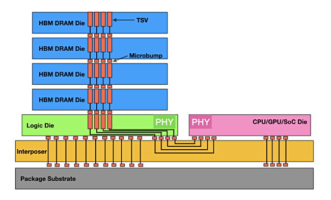
Think of HBM as a different way of combining memory chips and giving them closer and faster access to the CPU. The distance to the processor is only a few ㎛ units which helps speed data transfers.
HBM has developed across generations with HBM1, then generations 1 and 2 HBM2, and now HBM2 Extended (HBM2E.)
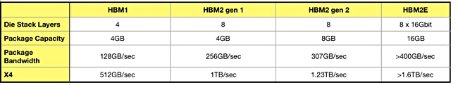
HBM2E is being developed. A Samsung Flashbolt HBM2E package offers 410GB/sec, 3.2Gbit/s per pin, and 16GB of capacity. SK hynix has gone beyond that with a 16GB package providing more than 460GB/sec.
The SK hynix package has a stack of 8 x 16Gbit chips and is rated at 460GB/sec.
Even this is slow compared to some other specialised forms of memory. Micron, for example, makes GDDR6 memory which pumps out data at 616GB/sec of bandwidth to a GPU. Micron is expected to bring out its own HMB2 product thus year.
SK hynix’s HBM2E package will be mass produced in 2020, which SK hynix expects to be a growth year for the HBM2E market.


