Home Blog Page 214

MRAM

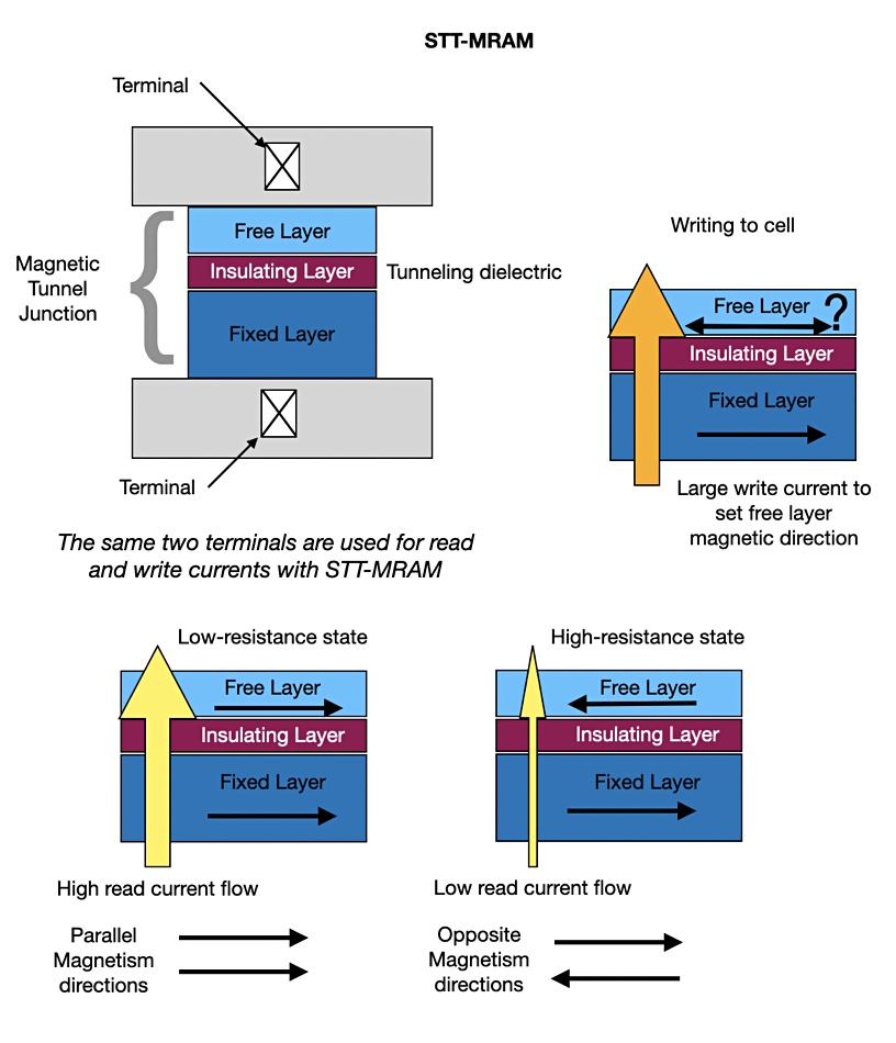
MRAM – Magneto-resistive RAM. It and STT-RAM (Spin Transfer Torque RAM) are the same thing: non-volatile and byte-addressable memory using spin-polarised currents to change the magnetic orientation, and hence bit value, of a cell. Crocus, Everspin and STT are the main developers here and they claim their technology has DRAM speed and can replace DRAM and NAND, plus SRAM and NIR, and function as a universal memory. But no semiconductor foundry has adopted the chip design for mass production and consequently the technology is unproven as practical SCM.

STT-MRAM diagram.
Everspin MRAM.
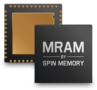
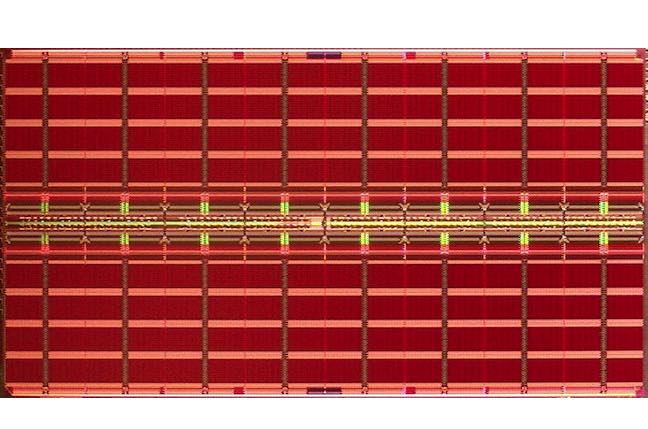
Spin Memory MRAM chips.

MAS-MAMR

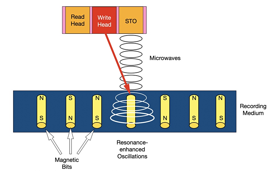
MAS-MAMR – Microwave Assisted Switching Microwave-Assisted Magnetic Recording. This is the use of resonance-enhanced magnetic oscillations between a spin-torque oscillator (STO) in the disk drive’s read/write head and the recording medium. The stronger oscillations facilitate writing data in narrower tracks in the media. MAS-MAMR drives capacity gains higher than FC-MAMR.

MAS-MAMR diagram.

MAMR

MAMR – Microwave-Assisted Magnetic Recording. This is a way of overcoming the thermal stability limitations of current Perpendicular Magnetic Recording (PMR) technology used in disk drives. PMR bits become unstable as their size shrinks below the 2TB/platter areal density point. MAMR records bits in a more stable but resistant recording medium, which needs beamed microwave energy to assist the read/write heads in writing bits.

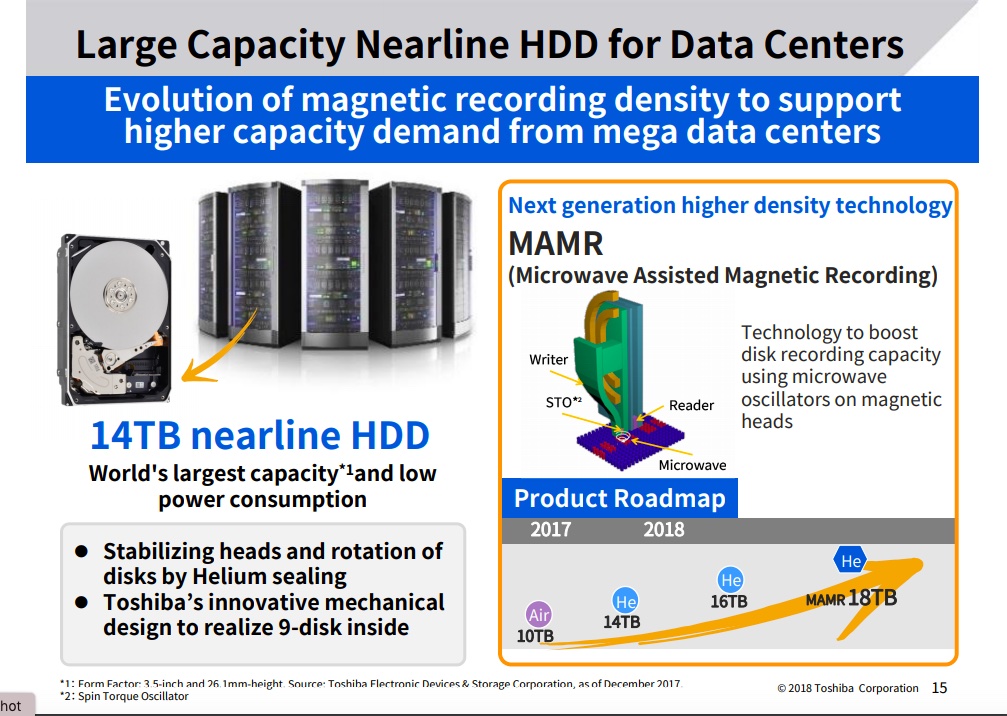
Toshiba diagram showing MAMR.

A MAMR-equipped write head has a main writing pole which projects magnetic energy or flux at the platter recording medium when it needs to write a bit. There is a space between the main pole and a trailing shield. A tiny Spin Torque Oscillator (STO) is inserted into this space. The STO has two components: a microwave Field Generation Layer (FGL) and a Spin Injection Layer (SIL).

M.2

M.2 – A small gumstick card-sized format used for flash memory drives. It can be single or double-sided and has a fixed size. The cards are described by 4- or 5-digit numbers which indicate their size. An M.2 2280 card is 22mm wide by 80mm long. The card widths and lengths can vary. M.2 cards fit into SATA or PCIe slots.

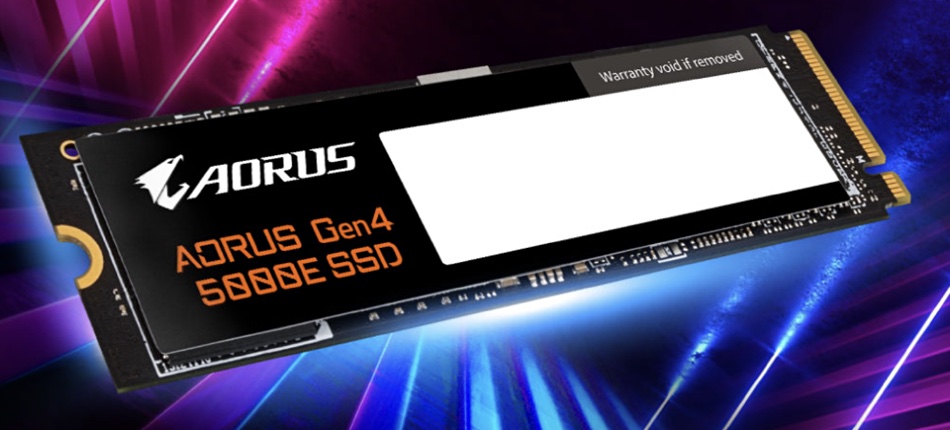
Gigabyte Aorus M.2 SSD.

MLC

MLC – Multi-Level Cell. The term is used to describe NAND with 2 bits per cell. Cells with 1, 3, 4 and 5 bits are called SLC (Single Level Cell), TLC (Triple Level Cell), QLC (Quad Level Cell)  and PLC (Penta Level Cell) respectively. Cells are read by using electrical voltages at various thresholds to detect the bit values. Here is how these multiple value cells work, with possible binary values for SLC, MLC, TLC, QLC and PLC cells being:

  • SLC = 0 or 1 – meaning two states and one threshold voltage,
  • MLC = 00, 10, 01, or 11 – four states and so three threshold voltages,
  • TLC = 000, 001, 010, 011, 100, 101, 110, 111 – eight states and thus seven threshold voltages,
  • QLC = 0000, 0001, 0010, 0011, 0100, 0101, 0110, 0111, 1000, 1001, 1010, 1011, 1100, 1101, 1110, 1111 – 16 states and so 15 threshold voltages,
  • PLC = 00000, 00001, 00010, 00011, 00100, 00101, 00110, 00111, 01000, 01001, 01010, 01011, 01100, 01101, 01110, 01111, 10000, 10001, 10010, 10011, 10100, 10101, 10110, 10111, 11000, 11001, 11010, 11011, 11100, 11101, 11110, 11111 – 32 states and so 31 threshold voltages.

Kioxia researchers devised  6-bit hexa-level cell flash (HLC) and 7-bit hepta-layer cell (HeLC) NAND in 2023. These are theoretical demonstrations for now.

The more bits a cell has the lower its endurance; its ability to have repeated write cycles before it wears out and stops functioning. For example, an SLC cell supports around 100,000 cycles while an MLC cell wears out after around 10,000 cycles. TLC is limited to 3,000 cycles. QLC supports about 1,200. A penta-level cells is likely to have less than 600 cycles, and so on for HLC and HeLC flash.
LUN

LUN – Logical Unit Number. This is used to identify an amount of block storage capacity in a SAN and may correspond to a part of or whole storage drive or group of drives.

LTO

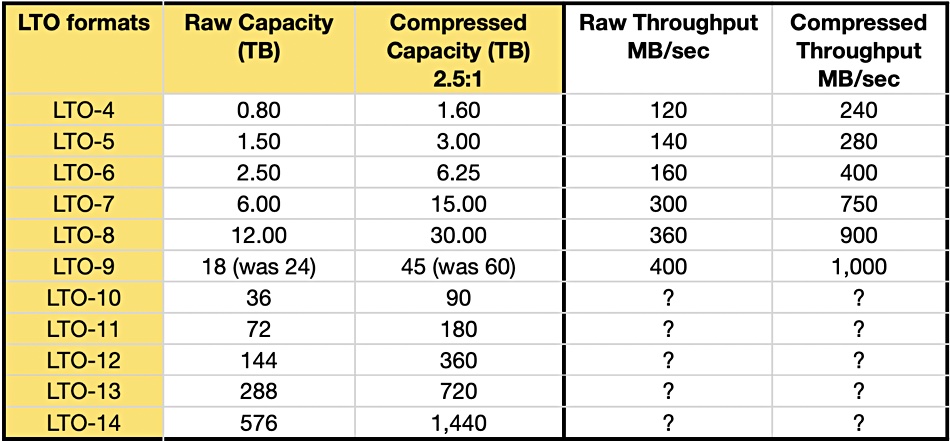
LTO – Linear Tape Open – a standard for tape storage controlled  by the LTO Program Technology Provider Companies – HPE, IBM, and Quantum. Only IBM makes the tape drives. It is currently in its ninth generation and has a roadmap out to LTO-14.

LTO generations and roadmap.
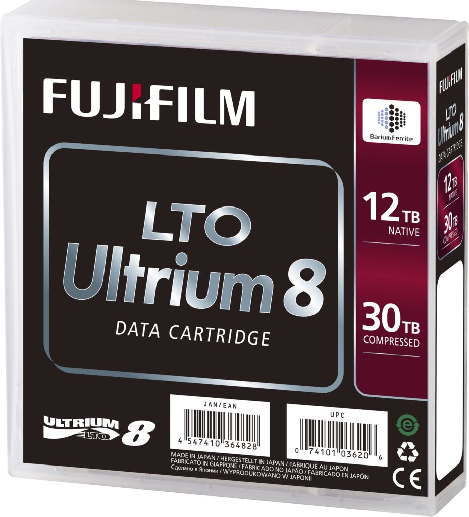
Fujifilm LTO8 cartridge.

LTFS

LTFS – Linear Tape File System. This presents a file:folder interface to LTO tapes. LTFS stores files and their metadata on the same tape and makes the data accessible through the file system interface. The LTFS standard defines the data recording structure on the tape and the metadata format in XML. It creates a full index when new files are added. V2.5 of the LTFS format specification uses a new and incremental indexing method with a journal-like capability where only changes to the index need to be recorded frequently. A complete index is required to be written at un-mount time.

Lock

Lock – A shared-access storage system needs some way to ensure that multiple actors working on the same file or region of a file cannot conflict by writing data at the same time, with one write preventing or corrupting the other. A lock prevents this. Before writing, an application or process will obtain a lock, from the filesystem for example, on the area it intends to modify; the whole file or a portion of it. While the lock is held, no one else can write data to the locked area. Once the write is complete, the lock is relinquished. This puts a burden on the system to manage locks. The then necessary process of obtaining, checking for, and relinquishing locks adds latency to every write transaction.  

LAN

LAN – Local Area Network. This term is used to describe a network within a data centre or building. It is also used to distinguish such a network from one crossing longer distances; a wide-area network or WAN. The main network protocol used in LANs is Ethernet. Every linked device in an Ethernet LAN has a unique 48-bit Media Access Controller (MAC) address. Data is sent out in packets with MAC addresses specifying the source and destination addresses of the packet.

Kilobibyte

Kilobibyte – 1,024 bytes. See Decimal and Binary Prefix entry.

Kilobyte

Kilobyte – One thousand bytes. See Decimal and Binary Prefix entry.