

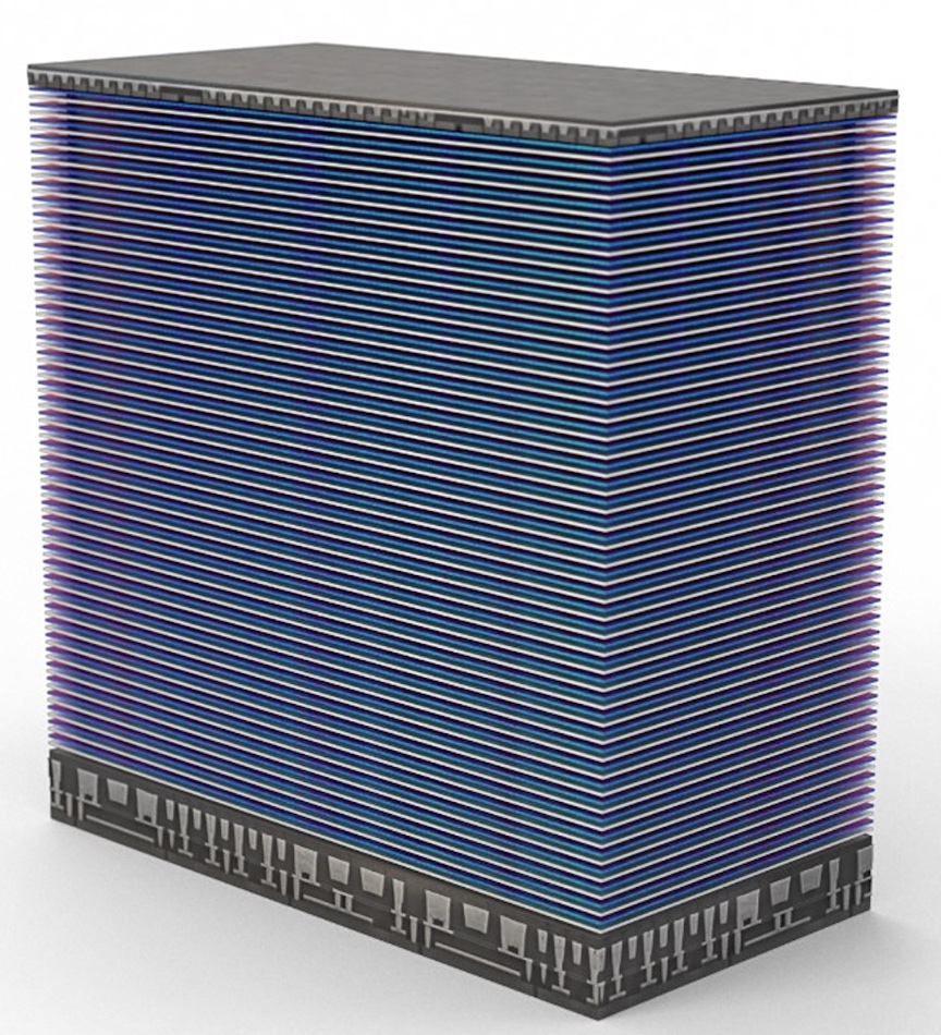
NAND – Not AND – a type of logic gate used in solid state drives which are built from flash memory chips. NAND flash is non-volatile memory, retaining its data when power is switched off, unlike DRAM. It is slower to read than NOR flash but faster to write. The drives are built from NAND chips which contain arrays of cells, originally built in a single layer but now manufactured in vertically stacked layers. This is called 3D NAND. A NAND cell consists of a device capable of trapping electrons in a particular location. The original way of doing this uses floating gate technology while a newer method used charge trap technology.
The presence or a sense of trapped electrons indicates a binary 1 or 0.
The floating gate is made from FGMOS or FGMOSFETs (Floating Gate Metal Oxide Field Effect Transistors) which are electronic components that can store either 0 or 1, indicated by electron presence or absence in the floating gate. NAND cells are read in pages or blocks, not individually. NAND cells are deleted in blocks by applying a voltage to a single wire connected to a group of cells, which are then erased in a ‘flash.’
NAND cells can store more than 1 bit of information by varying the read voltage level in a cell. SLC is 1 bit/cell, MLC is 2 bits/cell, TLC is 4 bits/cell, QLC is 4 bits/cell and PLC is 5 bits/cell.
- SLC = 0 or 1 – meaning two states and one threshold voltage,
- MLC = 00, 10, 01, or 11 – four states and so three threshold voltages,
- TLC = 000, 001, 010, 011, 100, 101, 110, 111 – eight states and thus seven threshold voltages,
- QLC = 0000, 0001, 0010, 0011, 0100, 0101, 0110, 0111, 1000, 1001, 1010, 1011, 1100, 1101, 1110, 1111 – 16 states and so 15 threshold voltages,
- PLC = 00000, 00001, 00010, 00011, 00100, 00101, 00110, 00111, 01000, 01001, 01010, 01011, 01100, 01101, 01110, 01111, 10000, 10001, 10010, 10011, 10100, 10101, 10110, 10111, 11000, 11001, 11010, 11011, 11100, 11101, 11110, 11111 – 32 states and so 31 threshold voltages.
Each added bit level slows the read speed and also shortens the cell’s working life or endurance.
A NAND chip is organised into blocks and each block is made up from a number of 4K byte pages. For example, a 128Gb NAND chip has 8,192 blocks of 128 pages each. NAND flash must be erased before it can be written, and erasing means putting all the cells in a block to the bit value 1. Then they can be written to a 1 (stay the same) or a zero.
Cells whose contents have been deleted are marked as invalid by a flash controller. The process of collecting valid cells from a partially invalidated block and writing them to a new block so as to leave a wholly invalid block behind is called garbage collection. When it is done the now empty old block is erased (all cells set to 1) and can be re-used.
