Kioxia engineers are presenting new DRAM storage-class memory and 3D-NAND technologies at the IEEE International Electron Devices Meeting (IEDM) 2024 conference in San Francisco, December 7-11.
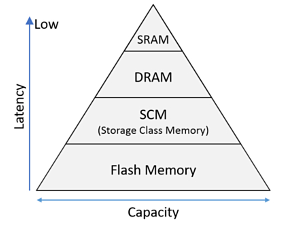
The company fabricates NAND chips in a joint venture with Western Digital. It makes no DRAM and has a fast FL6 SSD, which is classed as storage-class memory (SCM) but not as fast as discontinued Intel Optane technology. SCM occupies a level in the memory hierarchy between DRAM and NAND, designed, Kioxia says, “to handle larger data volumes than DRAM and at higher speed than flash memory.”

Kioxia says it will unveil a new type of DRAM utilizing oxide semiconductors with a focus on reducing power consumption, MRAM suitable for larger capacities for SCM applications, and a new 3D NAND structure with superior bit density and performance.
In the DRAM area, Oxide-Semiconductor Channel Transistor DRAM (OCTRAM) technology is being jointly developed by Nanya Technology and Kioxia. It features a gate-all-round InGaZnO (Indium Gallium Zinc Oxide) vertical transistor with the oxide reducing current leakage to an “extremely low” level. This transistor “enhances circuit integration by improving the manufacturing process,” and is described in Paper number 6-1 at the conference, Oxide-semiconductor Channel Transistor DRAM (OCTRAM) with 4F2 Architecture.
The 4F2 term refers to a DRAM memory cell in which the cell’s area is four times the square of the feature size (F). The paper abstract says this transistor design achieved “Ion=15uA/cell (Vg=2V) and Ioff=1aA/cell (Vg=-1V). A 275Mbit OCTRAM array was fabricated with WL 54nm/BL 63nm pitches and showed successful operation in the designed voltage range, making it a breakthrough technology for future 4F2 DRAM.”
A second conference paper, number 20-1, entitled “Reliable memory operation with low read disturb rate in the world smallest 1Selector-1MTJ cell for 64 Gb cross-point MRAM,” discusses MRAM-based storage-class memory being jointly developed by SK hynix and Kioxia. The two will say they “achieved cell read/write operation at the smallest-ever scale of cell half-pitch of 20.5 nanometers for MRAM by combining cell technology that pairs selectors suitable for large capacities with magnetic tunnel junctions, and applied fine processing technology for crosspoint-type arrays.”
To counter reliability degradation associated with miniaturized cells, the two used a “new readout method that leverages the transient response of selectors and by reducing the parasitic capacitance of readout circuits.”
The paper abstract states “demonstrate reliable 1 selector-1 MTJ (1S1M) cell read/write operation with low read disturb rate of <1E-6 in 64 Gb cross-point array architecture. We have implemented cross-point 1S1M chips integrated in Half Pitch (HP) of 20.5 nm and MTJ CD of 20 nm using As-doped SiO2 selector and perpendicularly magnetized MTJ (p-MTJ). A novel read scheme utilizing transient behavior of selector along with the low capacitance circuitry enables us to overcome MTJ read disturb easily occurred when the selector turns on in scaled 1S1M cells.”
Kioxia’s third event paper (number 30-1) is titled “Superior Scalability of Advanced Horizontal Channel Flash For Future Generations of 3D Flash Memory” and describes a new 3D structure to improve reliability and prevent cell performance degradation. It stacks the NAND cells horizontally instead of vertically as is the norm currently, and this counters the cell degradation that happens when the layer count increases too much in vertically stacked 3D NAND.
The paper abstract states: “We propose a novel architecture, advanced horizontal channel flash (HCF), that uses Local Block Interconnect, staggered Select Gates, and memory cells employing Floating Gate based charge storage. HCF with minimized 2F2 cell shows better cell efficiency than that of Vertical Gate NAND designs with 6F2 cell and of conventional 3D flash memory with 4F2 cell. Furthermore, HCF maintains the advantage of the VG-type devices, where cell current remains independent of the stacking number. The operation of the HCF device has been confirmed by TCAD simulation and a test vehicle fabricated using a 3D flash compatible process flow.”


