

Micron is sampling a 25GB high bandwidth memory product made from a stack of 8 smaller chips, just months after SK hynix’s 24GB, 12-high stack. The company also said it has a 36GB, 12-high HBM3 stack coming.
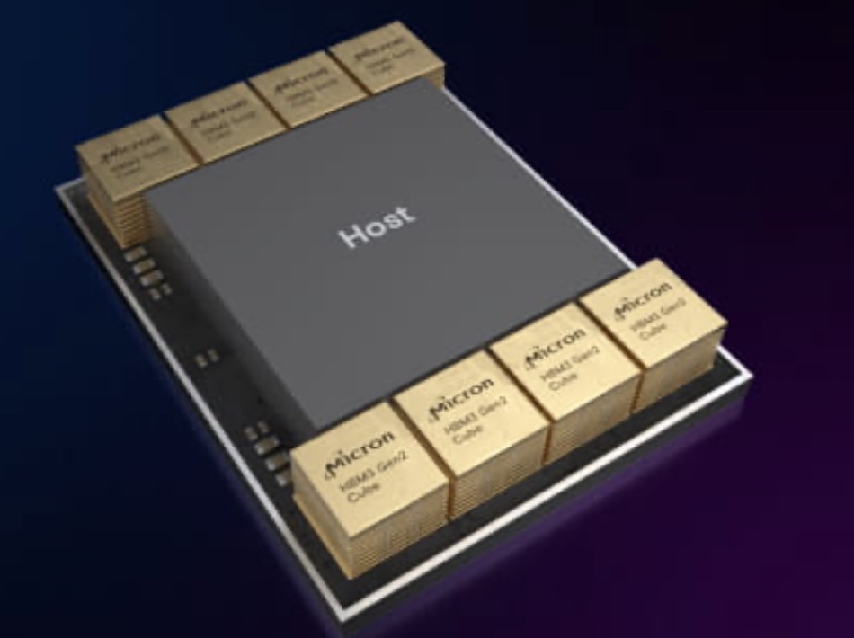
High Bandwidth Memory (HBM) is a way of combining multiple DRAM dies in a single chip and connecting this to a host CPU via an interposer. This enables a server to have more DRAM and higher bandwidth than can be obtained from the traditional but limited-in-number socket interfaces which hook up DRAM-carrying DIMMs to the processor. In effect a DIMM is replaced by a much larger HBM DRAM stack. GPU systems use HBM in preference to DIMMs because of their higher capacity and bandwidth.
Micron’s Praveen Vaidyanathan, VP and GM of its Compute Products Group, said: “Micron’s HBM3 Gen2 technology was developed with a focus on unleashing superior AI and high-performance computing solutions for our customers and the industry.”

The 24GB Micron product, built using its 1β (1-beta) DRAM process node, delivers more than 1.2TBps of bandwidth, using a pin speed faster than 9.2Gbps, which it claims is a 50 percent improvement over current HBM3 products. An SK Hynix HBM3 chip delivers up to 819GBps and that satisfies Micron’s 50 percent improvement claim.
Micron claims that, when using its new HBM3 product, the training time for large language models will be reduced by more than 30 percent, resulting in lower TCO. Also the product will benefit ML inference operations as it “unlocks a significant increase in queries per day, enabling trained models to be used more efficiently.“
All-in-all the sampling product “addresses increasing demands in the world of generative AI for multimodal, multitrillion-parameter AI models.”
Micron says its new HBM3 product – its second gen of HBM3 – is 2.5x better on a performance per watt rating than previous HBM3 products. It claims this has come about because of a doubling of the through-silicon vias (TSVs or connecting holes) over competitive HBM3 offerings, thermal impedance reduction through a five-times increase in metal density, and an energy-efficient data path design.
This should save datacenter electricity costs, with Micron claiming that, for an installation of 10 million GPUs, every five watts of power savings per HBM cube is estimated to save operational expenses of up to $550 million over five years. We’re talking about massive datacenters here.
Nvidia VP of Hyperscale and HPC Computing, Ian Buck, said: “At the core of generative AI is accelerated computing, which benefits from HBM high bandwidth with energy efficiency. We have a long history of collaborating with Micron across a wide range of products and are eager to be working with them on HBM3 Gen2 to supercharge AI innovation.”
Semiconductor foundry operator TSMC has received samples of Micron’s HBM3 Gen2 memory and is working with Micron on evaluation and testing.
Micron’s 36GB, 12-high stack, HBM3 gen 2 product will start sampling in the first calendar quarter of 2024.


