


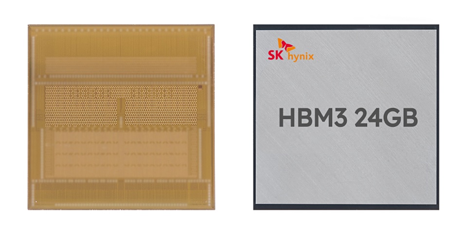
SK hynix has developed a high-performance, high-capacity high bandwidth memory chip composed of 12 DRAM chip layers bonded together providing 24GB of DRAM. It’s looking to sell them into compute-intensive markets such as the AI chatbot industry.
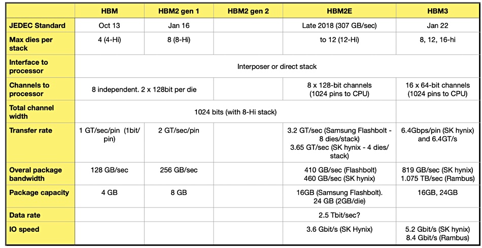
High bandwidth memory (HBM) has been devised to get around the x86 CPU socket scheme for hooking up DRAM to CPUs. A socket is effectively a channel and there are a limited number per CPU, 8 per Ice Lake gen 3 Xeons, providing about 200GB/sec of memory bandwidth. HBM, with a more direct, interposer-based, processor connection, has higher bandwidth – up to 819GBps with SK hynix’s HBM gen 3 scheme. SK hynix started mass production of an 8-layer HBM gen 3 chip in June last year with 16GB of capacity. Now it has moved on.
A spokesperson said: “The company succeeded in developing the 24GB package product that increased the memory capacity by 50 percent from the previous product. … We will be able to supply the new products to the market from the second half of the year, in line with growing demand for premium memory products driven by the AI-powered chatbot industry.”
There have been five HBM generations so far, with JEDEC standards defining them:
SK hynix fabbed the basic DRAM chips and used TSV (Through Silicon Via) interconnect technology, that provides thousands of holes through the chip, for electrode connections. This enabled the chip thickness to be reduced by 40 percent over its non-TSV-using predecessor. That, in turn, meant 12 chips could be stacked with the same height as its prior 8-layer, 16GB product; 50 percent more capacity in the same product dimensions.
The 12 DRAM layers were affixed together using Mass Reflow Molded Underfill (MR-MUF) technology, with which, SK Hynix says, multiple chips are stacked on a base substrate and bonded through reflow, simultaneously filling the gap between the chips or between the chip and the substrate with a mold material.
The reflow bonding involves two soldered parts pressed together and heated so that the solder melts and flows, and then cools to form electrical bonds.
Potential customers have evaluation samples of these 12-layer 24GB HBM chips, the highest capacity HBM3 chips available. Sang Hoo Hong, head of Package & Test at SK hynix, said: “The company plans to complete mass production preparation for the new product within the first half of the year.”
The intention and hope is that there will be a surge in enterprise adoption of large language model AI technology, like ChatGPT, which will boost GPU sales. GPUs needs lots of memory and use HBM technology for that rather than slower x86 CPU socket methods.
Step forward SK hynix with fast, high-capacity HBM3 chips ready and waiting to keep those bots chatting.


