


Kioxia has floated wafer scale SSDs as a much cheaper manufacturing method. As well as costing less than today’s data centre class SSDs, Kioxia says wafer-scale SSDs will deliver millions of IOPS.
But how does turning the wafer into an SSD affect performance and packing density?
Update: Jim Handy views on costs added. 14 July 2020.
Kioxia’s chief engineer Shigeo Oshima discussed the company’s ideas about wafer scale SSDs last month at the VLSI Symposium 2020 session. This was reported first in a Japanese media outlet but certain details are sketchy.
Comparative capacities
Blocks & Files has made some calculations on our trusty back of an envelope and we wonder how wafer-scale SSDs would be any better than ruler-format SSDs.
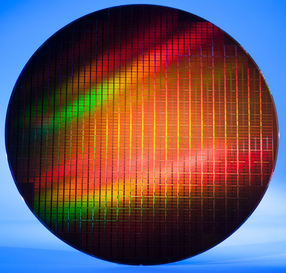
A NAND wafer is circular, 300mm in diameter, and holds a maximum of 700 dies. At the 200+ layer level these would be 512Gb dies in Samsung’s case. A wafer would hold 700 x 512Gb = 358,400Gb, which adds up to 44,800GB or 44.8TB.
Compare this to a 2.5-inch Samsung PM1643 SSD and Kioxia’s PM6 SSDs, which both hold 30.72TB.
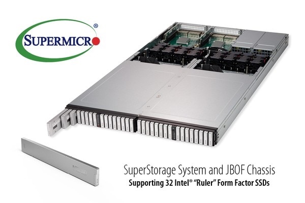
Upcoming ruler format SSDs are longer and slimmer than the 2.5-inch U.2 format SSD and and more can be packed into a 1U or 2U server box. For example, Intel’s EDSFF E1.L ruler is 325.35mm long, 9.5mm wide and 38.6mm high, holds 15.36TB. Thirty-two units fit across the front of a 1U rackmount enclosure, giving it 32 x 15.36TB capacity – 492TB.
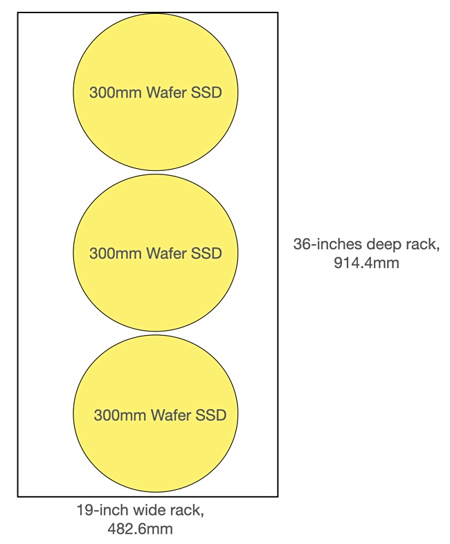
Rack packing density
A standard rack is 19-inches (482.6mm) wide, including the ears that fit either side onto the rack frame posts. Going crosswise, this means only one 300mmm diameter wafer-scale SSD can fit into the rack. The rack is 36-inches (914.4mm) deep, so two 300mm wafer SSDs could certainly be placed one behind the other, and possibly three if packed closely.
It’s easier to fit rectangular items into a rectangular box than circular items. As an analogy think about how vinyl records and DVDs came in oblong packaging to fit more easily into bookshelves and drawers.
Let’s compare the 1U Supermicro storage shelf above, with its 32 rulers, with a similar storage enclosure using two wafer SSDs in its front, and similar power, cooling and connectivity units at the rear of the rack shelf.
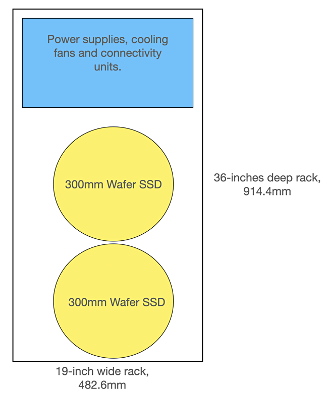
This 1.75 inches high 1U rack enclosure could hold more than two 300mm NAND wafers by stacking them. They would have to be cooled and, assuming 0.3 to 0.4-inch cooling air gaps between the wafers, you could stack four in 1U, so 4 x 44.8TB = 179TB.
Two stacks, one behind the other, gives us 358TB. By our guesstimate, the ruler SSD packing density is 27 per cent greater than the wafer SSD packing density. So wafer-scale SSDs appear to have a cost disadvantage when it comes to packing density.
Of course, acquisition cost is just one element of total cost of ownership, which also includes power, cooling and data centre space considerations.
Performance
A 30TB U.2 SSD using 512Gb dies would have 469 dies and the dies can be accessed in parallel. Kioxia’s Oshima said wafer-scale SSDs could deliver millions of IOPS and enormous performance. So-called “super multi-probing technology” would enable hundreds of chips on the wafer to be accessed at the same time.
In other words, the raw dies on the wafer would need IO access channels and a wafer-level controller to operate the wafer drive. In principle, this is what happens with SSDs today. IO channels are added to the dies, and connect them to a controller. The controller can access individual dies in parallel and so increase IO performance. This is limited by the bandwidth of the PCIe channel hooking up the drive to the host server’s memory.
To gain a performance advantage, wafer scale SSDs would require significantly more parallelism – and hence more IOPS and bandwidth – than an M.2, U.2 or ruler format SSD.
Costs
Jim Handy of Objective Analysis watched a recording of Oshima’s presentation. With reference to the wafer-scale SSD section he told us: “There wasn’t a lot of substance to that part of the presentation. In essence the speaker said that they can probe every chip on the entire wafer at once, and somehow this will allow SSDs to be built without any of today’s intervening steps between the wafer and a storage system.
“He said that this will allow costs to be reduced to “as little as” 20 per cent of the cost of today’s flash storage. He then points out that HDD’s cost is ~10 percent that of flash from which the audience would naturally conclude that HDD is threatened.
“The real crux of the story is how they can get the cost to that 20 per cent level. This is a little hard for me to understand since SSDs sell for as little as 9 cents/GB today, and the cost to make a wafer of 96-layer TLC is about half of that, or 4.5 cents. (64-layer TLC is closer to 6 cents.)
“If SSDs only cost twice as much as it costs to produce a wafer of NAND flash, then it’s hard to see how anyone would be able to get an SSD’s or even a flash array’s cost down to 20 per cent of current levels simply by reducing packaging costs”.
Net:Net
To conclude, we think wafer-scale SSDs are an interesting idea. But they have lower rackmount packing density than rectangular standard format SSDs. It is unclear how the merits of the technology as trailed by Kioxia, overcome this disadvantage. We have contacted the company and will update the article if we find out more.


