


Micron and Western Digital (WD) want some of the $280 billion US CHIPS and Science Act funding to go towards semiconductor research for memory-centric computing.
Update. WD replied with a ‘no comment’ type reply to our query about involvement with Micron and the MCOE. See the last but two paragraph. 9 Aug 2022.
The two are pushing for a Memory Coalition of Excellence (MCOE) funded by the National Semiconductor Technology Center (NSTC), which is being set up by the CHIPS and Science legislation funding. The arguments are outlined in a jointly authored report by memory maker Micron and storage vendor WD titled Memory Coalition of Excellence Recommendations for the National Semiconductor Technology Center.
Scott DeBoer, who runs Micron’s Technology and Products organization, writes: “Memory is not only ubiquitous, it is at the leading edge of semiconductor manufacturing, requiring production of advanced technologies that are pushing the laws of physics. … we now have a historic opportunity to regain global semiconductor leadership through the passage of the Chips and Science legislation and subsequent funding of the NSTC.
“The NSTC will be a public private-sector consortium focused on enablement of advanced semiconductor technology. It will play a pivotal role in driving US technological innovation and leadership over the long term. Furthermore, it will support the US in refining and accelerating its global technology and semiconductor leadership.”
Micron and WDwant the NSTC to focus on memory-related semiconductors: “The establishment of a Memory Coalition of Excellence (MCOE), as a pillar within the NSTC, is critical for foundational memory technologies and will further enhance American economic competitiveness and national security. The MCOE will bring together industry leaders, academia and national labs further supporting the US in refining and accelerating its global technology and semiconductor leadership.”
In DeBoer’s view: ”The NSTC should develop and articulate a long-term (>5 years) vision and roadmap for the future of next-generation semiconductor technology.” Some key activities for the MCOE are said to include:
- Research and development for materials, process/metrology technologies, and new analysis techniques
- Modeling methodologies and tools
- Next-generation 3D memory technology development
- New memory design concept enablement
- Near and/or in memory compute prototyping
- Heterogeneous integration at wafer and chip level
- Advanced packaging
The report
The 16-page MCOE report is recommended reading for anyone involved in NAND and DRAM development. There are 10 contributors, five from MIcron and five from WD. The WD contribution is all about NAND, not hard disk drives. WD has a joint venture with Japan’s Kioxia to make 3D NAND chips, and uses its half of the foundry’s output to make SSDs. WD has no NAND fabs in the US whereas Micron has two; one in Manassas, Virginia, and the other in Boise, Idaho.
The report says microelectronic chips and semiconductor technology are crucial for the US’s competitiveness: “Semiconductors play a pivotal role in US national economic activity and national security… The United States’ competitiveness in memory faces several challenges compared to other countries, including economies of scale and more limited investment incentives.”
It points out: “The cost of continually redeveloping and improving logic chips over the past decade has become exorbitant, limiting production capabilities to only a few of the world’s largest companies.”
It argues that the US government does not provide enough R&D help: “While the federal government accounts for 13 percent of total semiconductor R&D investment in the US, this percentage is well below the 22 percent average across all other technology sectors.” Therefore: “It is imperative for US federal investments to prioritize memory and storage R&D.”
“The ubiquitous nature of memory in electronic systems means that memory cells make up approximately 85 percent of the entire device count in semiconductor manufacturing. However, US-based manufacturing of memory only accounts for 2 percent of the global total… Federal initiatives, such as the proposed NSTC, provide a unique opportunity to support sustained domestic memory technology innovation, thereby bolstering US national and economic security.”
Micron has already pledged to expand its US DRAM/NAND fab infrastructure.
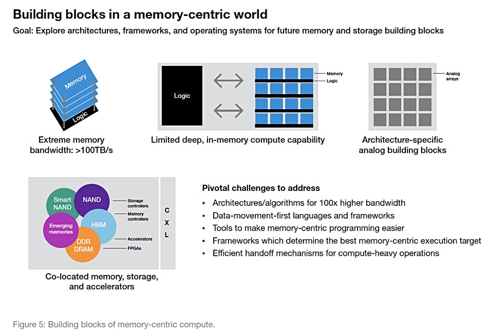
The bulk of the report deals with DRAM and NAND technology matters and declares that there is a memory wall holding back computing development: “Current data handling schemes rely on an architecture in which data storage is separate from data processing. This creates a need to constantly shuttle information to and from memory, which happens at great performance cost, in both time and energy. ‘The memory wall’ refers to this time and energy bottleneck in the system.”
Memory-centric architectures exist to bypass this memory wall:
- Computational storage
- Near-memory compute
- In-memory compute
- Analog accelerators
Analog accelerators are part of domain-specific architectures tailoring the architecture to characteristics of the workload. Each of these four items is increasingly efficient in terms of the energy needed per byte (picoJoules/byte or pJ/b):
The report says: “Memory and storage chip technologies have transitioned into a post-Moore’s law regime: the 3D scaling paradigm… Continued progress on this path requires a complete reimagination of the interaction between compute, memory, and storage.
“Memory-centric compute is the logical path to perform advanced computing at low energy and high performance for memory-bound workloads, including AI inference and training.
“Any serious move toward memory-centric compute requires integrated innovation from applications to the storage bits, including architectures, frameworks, operating systems, and memory systems. All items in the compute stack must evolve together in a system-level driven memory-centric paradigm.”
“Bringing workloads closer to memory has begun with stacking memory chips in a 3D fashion, termed high-bandwidth memory (HBM), and integrating these stacks with systems in a 2.5D manner… one can imagine the complete merging of memory and logic where analog memory functions are arranged to provide concurrent compute capability.”
What the report writers want is for the MCOE to “focus on pre-competitive research in materials, process, 3D structures and manufacturing technologies for memory and collaborate with other COE’s (Centers of Excellence) on packaging and interconnect technologies to enable next generation of energy-efficient computing and domain-specific accelerators… The MCOE should also identify a set of nation-wide grand challenges facing memory performance scaling that encourage large-scale collaboration across the US semiconductor ecosystem.”
The MCOE will be an institute with advanced facilities: “The facilities and infrastructure should provide advanced memory/storage, logic, and analog system prototyping with enablement of supporting materials, devices, and packaging. The envisioned infrastructure for such goals includes state-of-the-art, 300 mm clean room space with leading-edge semiconductor tooling capabilities to fabricate full-flow, concept memory chip prototypes, components and modules, as well as a dedicated systems lab for verification and testing”
The report writers think there should be “a fast ramp from lab to fab.”
Report conclusion
1. A concerted drive by the NSTC can accelerate innovation in memory and storage by enabling next-generation memory-centric design architecture, 3D memory structure technology development, and heterogeneous integration.
2. The NSTC should create a Memory Coalition of Excellence to support focused attention on the aforementioned memory-centric innovations needed for compute infrastructure of the future.
3. Investment in memory advancements will prevent semiconductor-based technology from stagnating and secure the continued cadence of technological advancements, thereby ensuring continued US economic and national security.
Western Digital involvement
Why is Western Digital involved? It has no fabs in China and therefore no danger of fab IP leaking. As far as we here at Blocks & Files can see, the only incentive is a closer relationship with Micron.
It is hard to see why the US government should fund domestic R&D to help give the WD-Kioxia JV access to new technology for its Japanese fabs. But if WD were to get closer to Micron, such as sourcing NAND chips or even building a joint fab in the US, that would be a different matter. We have asked Western Digital to comment and a spokesperson replied: “We appreciate your interest. We don’t have any further comment to provide. Everything we have to say on this matter is in the white paper.”
A no comment comment.
One other piece of background context: activist investor Elliott Management is pushing for Western Digital to separate its HDD and NAND/SSD operations into two separate businesses. WD’s board is examining strategic options for the corporation. One of these options may involve a closer alignment with Micron.


