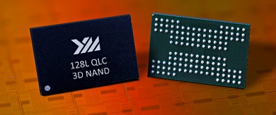
China’s Yangtze Memory Technology Corporation (YMTC) has begun sampling what it claims is the world’s highest density and fastest bandwidth NAND flash memory.
YMTC has developed the X2-6070 chip with a 1.333Tb capacity and 1.6Gbit/s IO speed using 128-layer 3D NAND with QLC (4 bits per cell) format. The chipmaker has also launched the X2-9060 chip with 512Gbit capacity and a TLC (triple-level cell) format from its 128 layers.

Grace Gong, YMTC’s SVP of marketing and sales, said the company will target the new QLC product at consumer grade solid-state drives initially and then extend the range into enterprise-class servers and data centres.
QLC is coming
Gregory Wong, principal analyst of Forward Insights, said in the YMTC press release: “As client SSDs transition to 512GB and above, the vast majority will be QLC-based. The lower read latency of enterprise and datacenter QLC SSDs compared to hard drives will make it suitable for read-intensive applications in AI, machine learning and real-time analytics, and Big Data. In consumer storage, QLC will become prevalent in USB flash drives, flash memory cards, and external SSDs.”
YMTC said the X2-6070 has passed sample verification on SSD platforms through working with multiple controller partners. We can expect several QLC and TLC SSDs using the X2-6070 and X2-9060 chips to launch in China, and possibly in other countries, between now and mid-2021.
With this launch, YMTC, a self-acknowledged newcomer to the flash memory industry, has joined the mainstream NAND vendors in developing 100+ layer technology.
The net result of their efforts is that SSDs using 100+layer 3D NAND in QLC format should ship from multiple sources in 2021.
A table shows how the vendors compare.

Xtacking
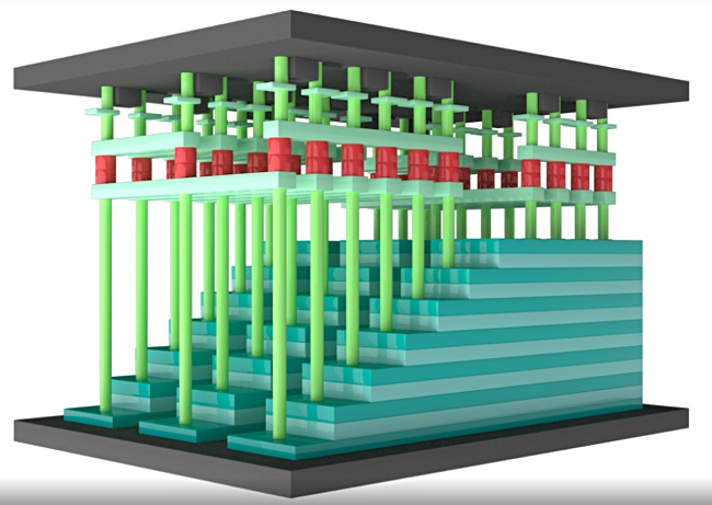
YMTC’s new chips use a second generation of the company’s proprietary Xtacking technology. This separates the manufacture of the NAND chips and controller chips, with each on their own wafers. The chips are attached electrically through billions of metal VIAs (Vertical Interconnect Accesses). The VIAs are formed across each NAND and controller wafer in one process step and the chips are then cut out. NAND chips and controller chips are mated so that the VIAs line up (shown by the red pillars in the diagram below).

There are two benefits to this design, according to YMTC. First, the chip area is reduced by 20 to 30 per cent because the peripheral controller logic is not placed on one side of the chip, as is otherwise the case. Secondly, the controller logic can be developed in parallel with the NAND die and this saves three months of development time, according to YMTC.
YMTC’s current NAND chip has 64 layers and we understand that the 128-layer chip is in effect two 64-layers, stacked one above the other in a string-stacking scheme. The 64-layer chip also uses Xtacking to put the controller logic above the NAND cells. YMTC’s 128-layer chip uses a second generation of Xtacking technology.
Layer cake
As well as YMTC, other suppliers also place the NAND die’s peripheral circuitry under or over the 3D NAND cells. For example, Samsung’s Cell over Peripheral architecture, arranges the bit-storing cells on top of the CMOS logic needed to operate the die. Intel and Micron have similar CMOS-under-Array designs.
SK hynix is preparing the 16TB 128-layer TLC PE8111 SSD in the EDSFF IU long ruler format, with sampling due in the second half of the year. A 32TB product will follow, but we don’t have a sampling date. Both chips use a 1Tbit die.
In January Western Digital and Kioxia announced 112-layer 3D NAND, with early shipping dates pegged at Q4 2020. BiCS5 technology will be used to build TLC and QLC NAND.
In December last year Micron said it was developing 128-layer chips with replacement gate (RG) technology. Gen 1 RG technology will start production in the second half of 2020, with slightly lower-cost chips. A gen 2 chip that brings in more layers, lower costs and a strong focus on QLC will appear in fy2021.
Last September Intel said it will move from 96-layer to 144-layer 3D NAND and will ship 144-layer SSDs in 2020. This is likely to be a pair of 72-layer string stacks.


