


Samsung revealed it is planning 280-layer QLC 3D NAND SSDs via an International Solid-State Circuits Conference (ISSCC) agenda.
The ISSCC conference will be held in San Francisco and a February 20 session presented by Samsung staff is entitled “A 280-Layer 1Tb 4b/cell 3D-NAND Flash Memory with a 28.5Gb/mm² Area Density and a 3.2GB/s High-Speed IO Rate.”
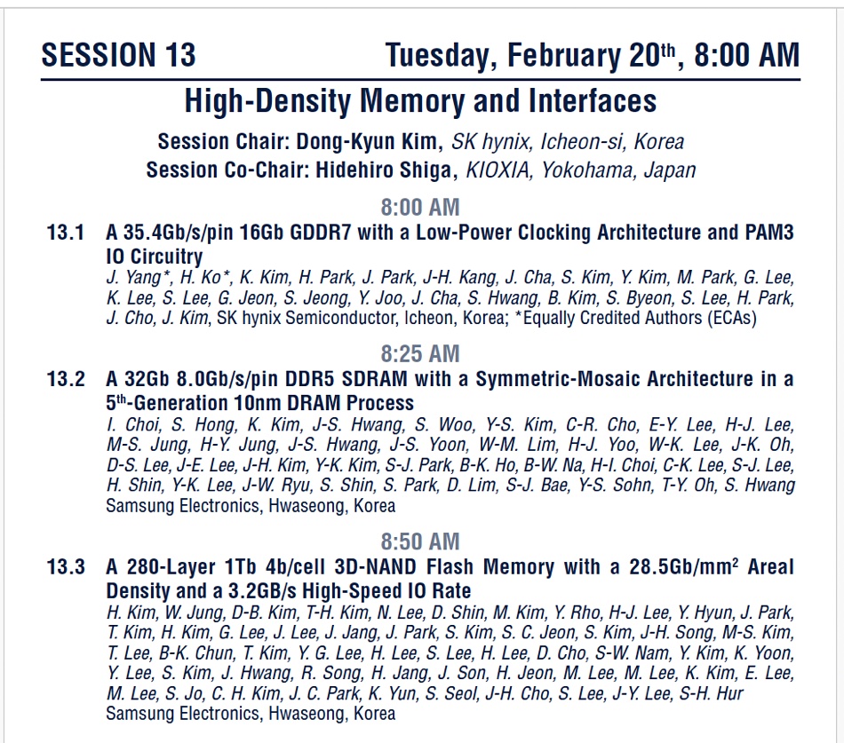
As reported by Germany’s ComputerBase, Samsung’s new V-NAND gen 9 flash has 280 layers, not the 300 previously associated with this generation. It’s a QLC (4bits/cell) technology and has, Samsung claims, industry-leading density of 28.5 gigabits per square millimeter as well as a fast IO rate for QLC flash.
UFS fingernail cards and M.2 gumstick cards will benefit from the higher density of these flash chips, given their limited physical space. YMTC has a 1 Tb QLC chip with a density of 20.62 Gb/mm² at 232 layers, while Micron’s density is 19.6 Gb/mm² using 232 layers, and WD/Kioxia is at the 13.86 Gb/mm² level with 162 layers. SK hynix has a 512 Gbit QLC chip with a 14.40 Gbit/mm² density at 176 layers.
Increasing the layer count is the key to increasing a chip’s density in Gb/mm² terms. At 280 layers, Samsung has the highest layer count flash, with SK hynix next at 238 layers, YMTC and Micron with 232, followed by WD and Kioxia with 218. SK hynix says it has a 321-layer chip coming next year. That could well give it a density edge until the other suppliers catch up.

A Tom’s Hardware report suggests that this Samsung flash could even enable 16 TB M.2 SSDs. That seems fanciful as current M.2 drives top out at the 2-4 TB level e.g. Sk hynix Platinum P41 at 2 TB, Seagate FireCuda 530 at 2 TB, Samsung 990 Pro at 4TB, and Micron 7400 Max M.2 at 3.2 TB. A jump to 8 TB might be feasible but 16 TB seems like a stretch too far.


