


Like any solid-state technology, 3D NAND will reach a point when it can’t meet demand for increased density, and replacement technology will come along. Semiconductor and nanotechnology research powerhouse IMEC reckons the answer will lie with Trench 3D NAND.
IMEC, the Interuniversity Microelectronics Centre, is a non-profit R&D institute with 4,000 research staff headquartered in Leuven, Belgium, and a track record for shrinking electronics to increase compute and memory performance.
An article from the institute, titled “The role of 3D-NAND-Flash and FeFET in the data storage roadmap” discusses how semiconductor elements like NAND cells are shrunk in the x, y, and z (length, width, height) dimensions to make the cells smaller so more can be built on a wafer to make denser chips and thus lower-cost or higher-capacity devices.
3D NAND
3D NAND was a response to scaling down limitations of planar NAND technology, which was based on floating gate transistors – floating, because its threshold voltage changes as the cell is written with a binary value and electrons flow across it. Planar, or 2D NAND, cell dimensions were progressively shrunk from 120nm, but from the 20–15nm level access speed decreases, the read error rate goes up, and program/erase (write) cycle number goes down – all because there basically aren’t enough electrons available to keep the cell’s state stable.
With 3D NAND, the planar cells were flipped from a horizontal to vertical orientation and strings of them built to form 3D layers. At the same time the cell dimensions were increased to to 30–50nm, with a 140nm x–y pitch, thus increasing the number of electrons per bit and making cells easier and faster to read and have a longer life.
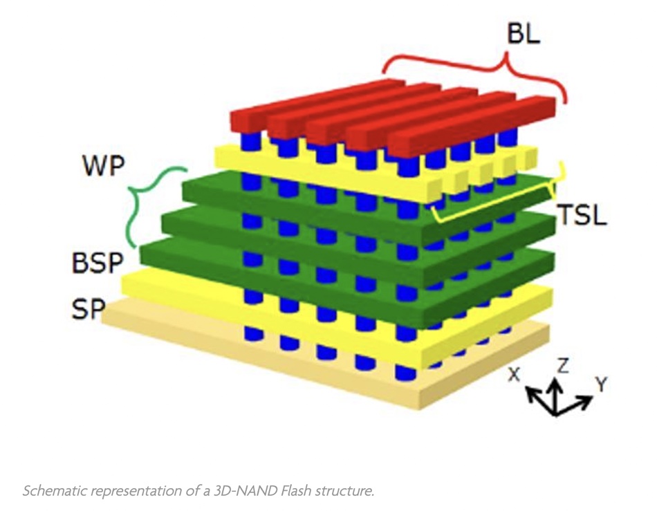
NAND chip density (capacity) can be increased by adding more layers, and the layer count has gone up from 12 through 24, 32, 468, 64, 96, 112, and is now at the 144 and 176-layer levels – depending on the manufacturer – with 200+, 500+, and even 1,000 layers in prospect.
3D NAND also increased density by adding bits to a cell, starting from single-layer cells (SLC) to 2-bit multi-layer cells (MLC), 3-bit triple layer cells (TLC), 4-bit quad-layer cells (QLC), and 5-bit penta-level cell (PLC) technology in development.
The counter to development in this fashion is that each step upwards in layer count prolongs production of the wafer. A hole etched through 64 layers is easier to do than 112 and 144 layers – the deeper the hole, the harder it is to etch consistently.
The foundry tools needed to deposit the layers of chemicals and etch out holes have to become more capable and complex as layer counts increase, adding to cost. There can be stress-induced errors in cells as layer counts increase as well, so finer, more precise production control is needed.
The difficulty at 200+ layers will be commensurately greater and larger again at 500 or more layers. String-stacking – placing two blocks of 3D NAND chips one above the other to bypass this problem – has already been done by some manufacturers, with, for example, a 128-layer device built from two 64-layer components.
But string-stacking delays the inevitable. Some time in the future the extra production difficulty will make it cost-prohibitive to go to the next layer count. At that point, the IMEC authors suggest, the NAND cells will have to get smaller again to enable denser chips to be built and so increase drive capacity and/or lower electricity consumption and ease cooling.
The authors suggest we could see “stacks of 1,000 layers being unavailable until 2030” unless new technology is explored.
Trenching
Generally speaking, 3D NAND has a cylindrical gate-all-around (GAA) design, and shrinking the cell size would mean component layer thicknesses and height would be reduced, threatening the ability of the cell to meet performance, stability, and longevity requirements.
The IMEC authors suggest a trench-like architecture in which “the memory cells are no longer circular. They are implemented at the sidewall of a trench, with two transistors at opposite ends of the trench, which significantly increases bit density.”
They write: “From an operation point of view, this trench cell resembles a planar unit cell (being put upright) compared to the circular GAA NAND-Flash cell.”
In their view, “Although it comes with a slight penalty in electrical characteristics (such as the program/erase window), the unit cell area in a trench-like configuration can be reduced in the x–y direction compared to a ‘GAA’ cell. As such, the trench cell is put forward as a next generation NAND-Flash cell architecture – expected to reduce the x–y pitch from today’s 140nm (effective) to about 30nm.”
Ze height is ze problem
Reduction in the z-dimension (height) may need material changes. “A z-shrink of the NAND-Flash layer stack involves squeezing the materials that are used for creating the word-line layers, including the word-line metal.”
They write: “Reducing the word-line metal thickness comes along with an unwanted resistivity increase, which enhances resistance-capacitance (RC) delay and slows down access times. IMEC, therefore, is looking at alternative metals such as Ru (Ruthenium) and (barrierless) Mo (Molybdenum) with potentially lower resistivity at small dimensions.”
IMEC researchers are “exploring alternative materials for the charge trap layers, the tunnel dielectrics and the metal gate stack, and … investigating their impact on memory performance.”
It’s a whole lot of work-in-progress and the NAND foundry folks and their in-house research engineers have to be involved as well –; they get to make the NAND wafers, after all.
If you are interested further then read the paper – there’s lots more in it.


