


Extended high-bandwidth memory (HBM2E) is barely here, yet Rambus already has a third-generation HBM subsystem ready for use, and it goes more than twice as fast.
Server and GPU memory capacity and speed is set to rocket up from today’s socket-connected X86 server DRAM. NVIDIA GPUs have already abandoned that and are using HBM — stacked memory dies connected to physically close GPU using an interposer instead of socket channels.
We can view an HBM+interposer+processor system as a using chiplets, with the HBM part being one chiplet, and the processor another, both connected via the interposer.
HBM stacks memory dies one atop another to increase package capacity beyond a DRAM DIMM and uses a set of wide channels to break socket connectivity limitations. Intel’s Ice Lake generation of server processors supports eight sockets, up from its preceding Gen-2 Xeon’s 6. That’s not enough for multi-GPU servers and developing analytics and machine learning models which need huge amounts of data stored in memory for fast and repetitive access.
The JEDEC standards organisation has created three HBM standards: HBM, HBM2 and HM2E, with E standing for extended. Each one of these increases performance and capacity beyond the prior generation, as a table shows:
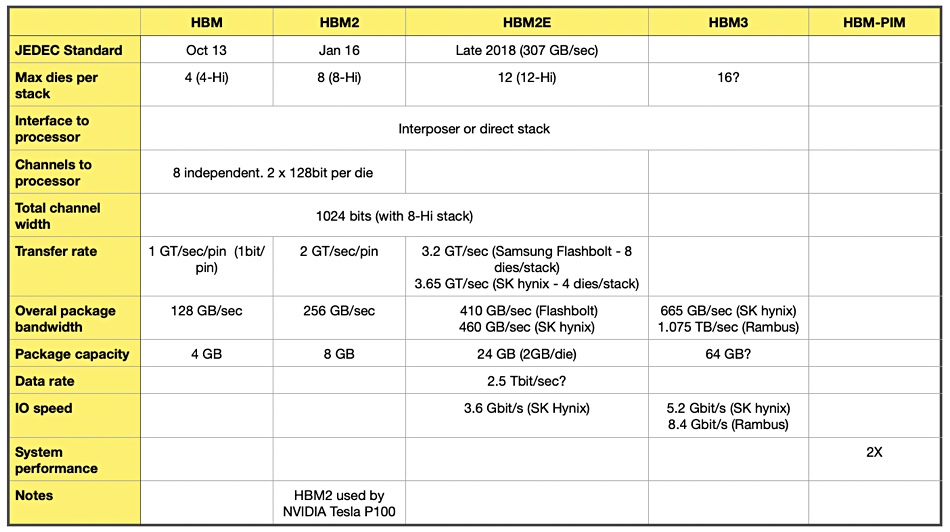
HBM3
The memory fabrication industry is pushing its technology boundaries beyond HBM2E with a third HBM generation: HBM3. There is no JEDEC standard for this as yet, although we understand JEDEC is working on one.
There are three HBM memory die suppliers: Micron, Samsung and SK hynix. SK hynix has discussed its HBM3 technology. Micron talked about “HBMnext” in August last year, saying it could have 4-Hi and 8-Hi stacks and a 3.2Gbit/sec data rate. That sounds like an HBM2E-class technology.
Samsung has ideas about putting processing elements directly into memory (PIM) to speed computation, and details of this technology are yet to emerge. It would be proprietary to Samsung. We have yet to hear from Samsung about its views on HBM3.
Rambus
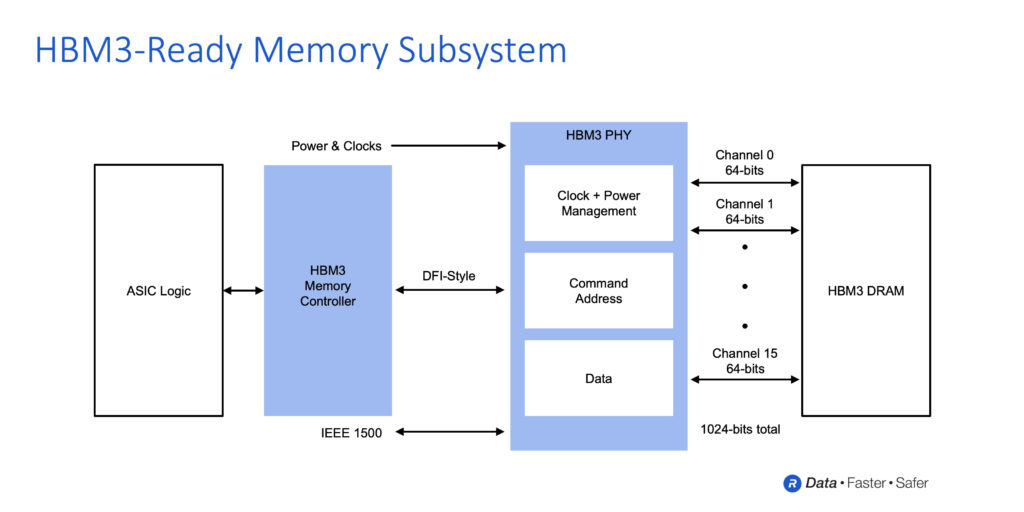
Rambus has produced an HBM3 interface subsystem consisting of a PHY (physical layer in OSI model) and digital controller. This subsystem supports an up to 8.4Gbit/sec data rate, way beyond SK hynix’s 5.2Gbit/sec HBM3 data rate, as seen in the table. It delivers 1.075TB/sec of bandwidth, beating SK hynix’s 665GB/sec.
The Rambus PHY+Controller combo is accompanied by 2.5D interposer and package reference designs to help memory system designers develop products faster.
AN IDC associate VP, Soo Kyoum Kim, provided a context quote for Rambus’s announcement: “The memory bandwidth requirements of AI/ML training are insatiable with leading-edge training models now surpassing billions of parameters. The Rambus HBM3-ready memory subsystem raises the bar for performance enabling state-of-the-art AI/ML and HPC applications.”
There are huge implication for overall system performance and design here. We could, possibly, see the replacement of socket-connected DRAM DIMMS by HBM. We could see HBM as a new, faster-than-basic-DRAM in the memory-storage hierarchy. Our sister publication The Next Platform has suggested that Optane could then replace DRAM in the hierarchy.
We could then see X86-GPU servers with extremely large memories capable of running analytical and machine learning model development workloads orders of magnitude faster than today. The Rambus and SK hynix HBM3 technology glimpses suggest a tantalising future.


