Suppliers and JEDEC are bringing their HBM4 plans forward as they suspect the forecasted Gen AI boom means incoming Nvidia GPUs will need it sooner.
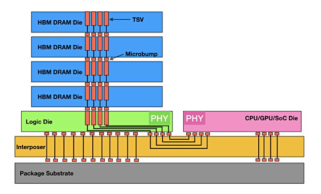
High bandwidth memory (HBM) bypasses X86 socket-connected DRAM capacity and bandwidth limits by having memory dies stacked on top of a logic layer, with interconnecting TSV channels, all linked to a GPU via an interposer component providing higher bandwidth than X86 sockets. The Joint Electron Device Engineering Council (JEDEC) confirms and issues HBM standards, with the current one being its fifth, HBM3E (extended).

The main HBM suppliers are SK hynix, followed by Samsung and then Micron. In April SK hynix saw first 2024 quarter revenues soar 144 percent due to HBM chip demand from Nvidia, which packages them with its GPUs. TrendForce says the HBM market is poised for “robust growth,” driven by pricing premiums and increased capacity needs for AI chips.
Micron is building 24 GB HBM3e chips, with 8 x 3 GB stacked DRAM dies (8-high), for use by Nvidia in its H200 Tensor Core GPUs. It also has a 12-high device with 36 GB capacity and >1.2 TBps performance. Samsung has its own 12-high, 36 GB HBM3e device, with up to 1.28 TBps bandwidth.
JEDEC has said it will issue a completed HBM4 spec by the end of this year – just few months ago the schedule was for a 2025 delivery. Preliminary HBM4 characteristics are emerging already.
An HBM4 controller will able to control HBM3E DRAM. HBM3E chips have a 1024 bit wide channel which HBM4 doubles to 2048 bits. The maximum number of stacked DRAM dies with HBM3E is 12. HBM4 increases that by a third to 16, with both 24 Gb and 32 Gb layers supported. This will give a boost to both capacity, with up to 512 Gb (64GB) supported, and bandwidth up to 6.4 GTps, meaning the host GPU can get more data faster, and so process bigger large language models.
A 16-high stack is, obviously, higher than a 12-high stack and JEDEC is considering increasing the HBM chip maximum height parameter from 720μm to 775μm. One way to reduce the height is to move to smaller process technology.
TSMC and SK hynix originally planned to use a 12nm 12FFC+ process but are now intending to add 5nm N5 process technology. Samsung says it is going to use 4nm technology for its HBM4 logic die, which will increase the die’s performance and lower its power consumption compared to the 10nm process used for its HBM3E chips.

A direct HBM-to-GPU connection, obviating the need for an interposer component, would shorten the distance between DRAM and GPU, speeding data access. However thermal design limits could prevent HBM4 stacks being bonded directly to a GPU. Two warm devices could make a single hot one difficult to cool.

Whatever the outcome of these issues we can be confident that the fierce competition between SK hynix, Samsung and Micron will produce GPU systems with HBM4 accessing more memory faster and making Gen AI LLM development both more affordable and able to scale out to larger models.


