


Japanese microcontroller embedded flash design company Floadia has developed a 7bits/cell — yes, an actual seven bits per cell — NAND technology that can retain data for ten years at 150°C, that will be used for a AI Compute-in-Memory (CiM) operations chip. Its use in SSDs looks unlikely.
The company’s announcement specifies analog data, but also says it is a 7bits/cell structure — which means digital data. Perhaps there is a “Lost in Translation” effect here. It also says that without its semiconductor design tweaks, a cell would only retain data for 100 seconds. How long its tweaked-design cell could retain data at room temperatures is not revealed.
This 7bits/cell technology is based on Silicon-Oxide-Nitride-Oxide-Silicon or SONOS-type flash memory chips developed by Floadia for integration into microcontrollers and other devices. Floadia said it optimised the structure of charge-trapping layers — ONO (oxide-nitride-oxide) film — to extend the data retention time when storing seven bits of data.
Its announcement says “the combination of two cells can store up to eight bits of neural network weights” which sounds odd. If one cell can store seven bits why shouldn’t two cells store 2 x 7 bits?
The CiM chip stores neural network weights in non-volatile memory and executes a large number of multiply-accumulate calculations in parallel by passing current through the memory array. Floadia says that makes it a good fit for edge computing environment AI accelerators because it can read a large amount of data from memory and consumes much less power than conventional AI accelerators that perform multiply-accumulate calculations using CPUs and GPUs.
It claims that its intended chip, despite a small area whose exact size is not revealed, can achieve a multiply-accumulate calculation performance of 300 TOPS/W, far exceeding that of existing AI accelerators.
Floadia is not revealing the capacity of its CiM ship’s NAND. A 2020 International Symposium on VLSI Design, Automation and Test paper, “ A Cost-Effective Embedded Nonvolatile Memory with Scalable LEE Flash-G2 SONOS for Secure IoT and Computing-in-Memory (CiM) Applications” may reveal more, but it is behind a pay wall.
SONOS is a charge-trap mechanism, trapping electrons in Silicon Nitride film. The retention life is controlled by optimising the thickness and film properties of oxide and/or Silicon Nitride films. The company’s website states: “SONOS is free from leakage of electric charge through defect or weak spots in the Bottom Oxide film caused by damage during Program and Erase operation, because trapped charges are tightly bonded with the trap site in Silicon Nitride Film.”
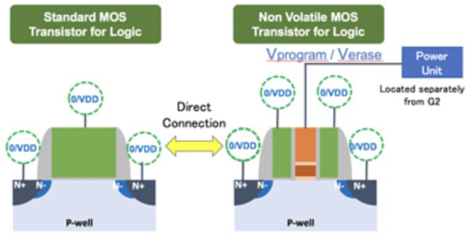
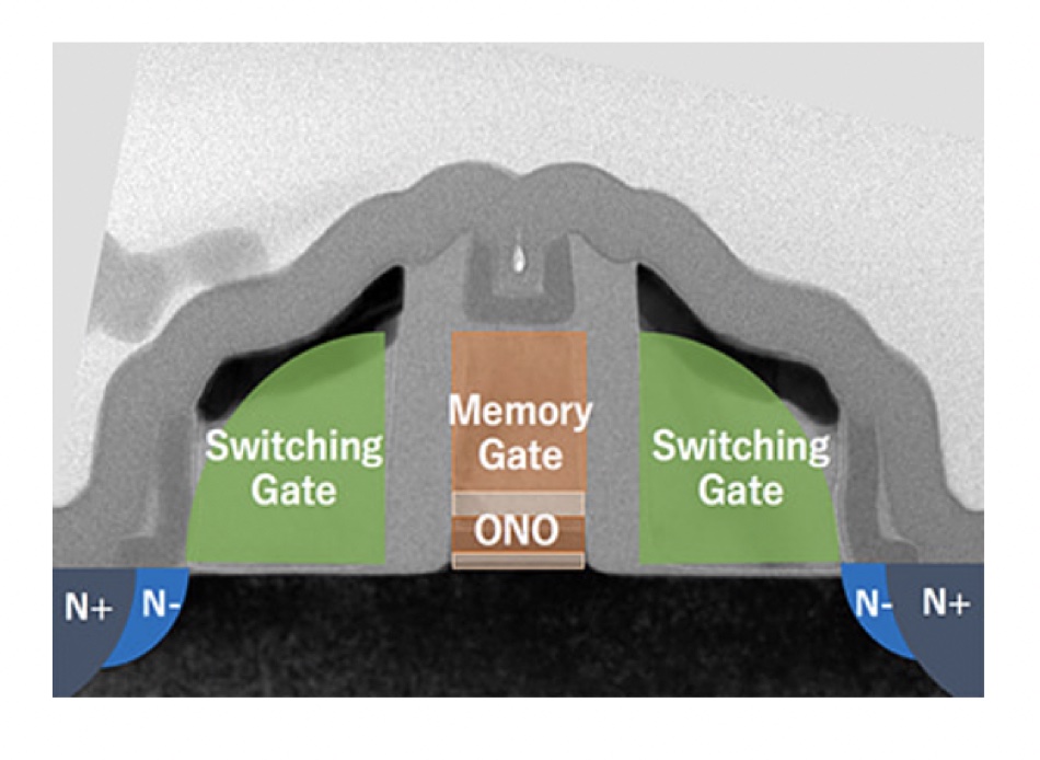
Also the “G2 cell consists of one SONOS transistor and two switching transistors placed adjacent to the SONOS transistor (see image above). This tri-gate transistor works as one Non-Volatile transistor operated by logic level voltage to switching transistors and high voltage only to the SONOS memory gate. Because of quite low programming current — pA order to each cell which is equivalent 1/1,000,000 of Floating Gate NVM — the wiring to the SONOS memory gate is treated like a signal line. And the power supply unit is able to be placed outside of the memory block — such as a corner area of the die. This unique feature of G2 provides LSI designers freelines of chip design and creation of new circuits combining logic circuits with Non-Volatile functionality.”
Floadia says the technology also uses Fowler Nordheim (FN) tunnelling technology to achieve extremely low power in program and erase operations, consuming 1/1,000,000 times current compared to conventional technologies using hot carrier injection for program/erase operation. It says: “G2 satisfactory supports operating temperature up to 125°C and 20 years of data retention life at 125°C.”
So we have 10 years at 150°C and 20 years at 125°C, which suggests retention periods at room temperature could be immense.
Whether this technology could be used in commercial SSDs is an interesting question and we’re asking a non-volatile memory expert, Jim Handy, about it.
Jim Handy’s view
Jim Handy of Objective Analysis told us “The first thing that I thought of when I saw your note was the company Information Storage Devices (ISD), which was acquired by Winbond in 1999. ISD made floating-gate chips that stored linear voltages to better than ±1 per cent accuracy (that would be around seven bits, if it were digitised). They got designed into lots of measurement equipment and into record-your-own greeting cards. My favorite application was an instrument to measure and record the stresses on bridges.
“Move ahead a couple of decades and you have Floadia doing the same thing, but a charge trap version targeting a different application: AI.
“It’s a good use of these technologies, and there’s a lot to be said in favour of making neural calculations in the linear, rather than digital, domain. AI can overlook noise and variations that add cost and complexity to digital implementations, and it’s trivial to perform multiplication and sums (linear algebra) in linear electronics at a high speed using very little energy.
“Floating gates and charge traps store voltages, and the use of MLC, TLC, and QLC has given developers a very good understanding of how best to manage that.
“As for using this in SSDs, that’s a different matter. If a flash chip didn’t need to run fast and be cheap then we may already have seen 7-bit MLC.
- Fast: There’s a lot of sensitivity to noise when you’re trying to digitise multiple voltage levels, but if you average over time then you can manage that, if you have a lot of time. Who wants a slow SSD?
- Cheap: You can store more precise voltages with a big charge trap than with a small one (likewise for floating gates). The bigger the bit, the fewer you get onto a wafer, so the higher the cost.
“But the whole point in going from SLC to MLC to TLC to QLC is to reduce costs. You wouldn’t do that by increasing the size of the bits.”
That’s a “No” then.


