


DRAM is expensive, and servers have limited capacity through their socket architectures, but we need more DRAM as processors get more deeply involved in working on larger and larger datasets for applications like AI and analytics. High Bandwidth Memory (HBM) and four other approaches are being explored to solve the problem and increase DRAM’s areal density: cell flipping, modified NAND-cells, floating body cells, and gain cells.
They’re examined in a Semiconductor Engineering article entitled “Will Monolithic DRAM Happen?” We look at the cell flipping idea here. The other concepts seem less well advanced for now and we’ll set those aside.
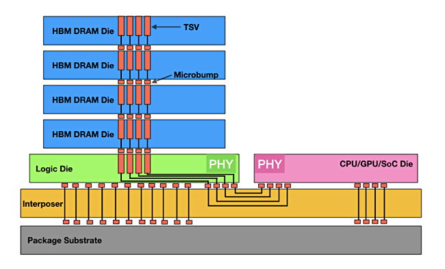
We have looked at HBM in several articles. It involves stacking 2D Planar DRAM dies in layers of up to eight dies, interconnected with wire holes called Through Silicon Vias (TSVs) and connected via microbumps to an interposer chip which similarly connects to an adjacent processor. This architecture limits the number of stacks that can be hooked up to a processor.
DRAM cell flipping
The 3D NAND concept involved changing the orientation of NAND cells to enable layers of them to be stacked inside a die.
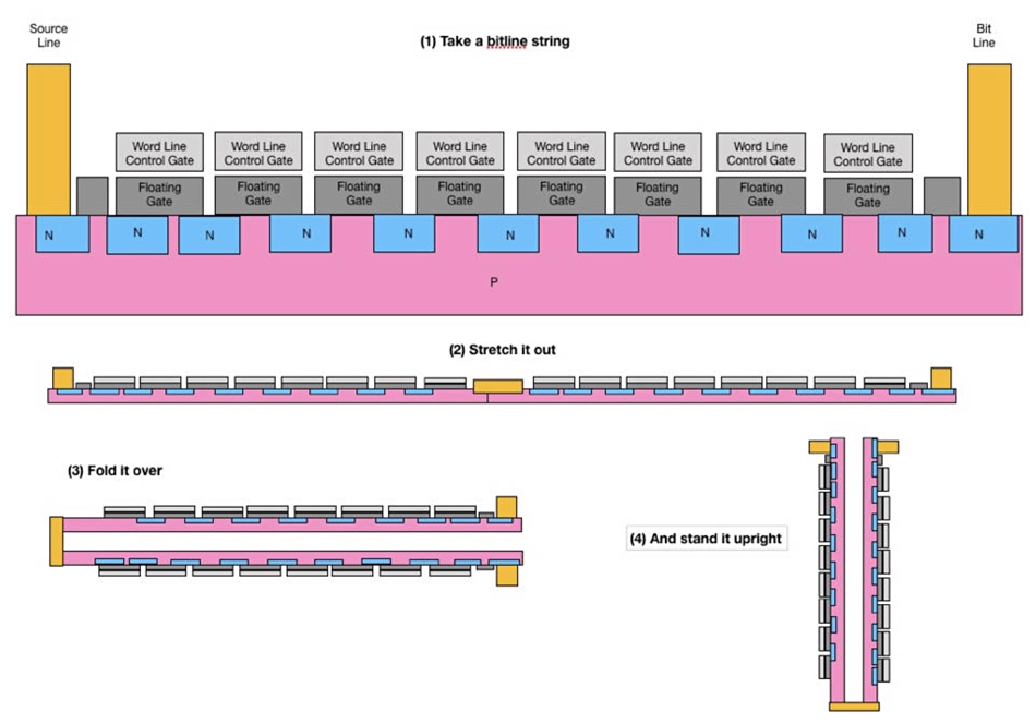
We can conceptually do a similar thing with DRAM — flipping the cells on their side. A DRAM cell has a small 2D area but a large, vertically oriented capacitor, making it high and difficult to stack in layers. As the 2D dimensions get smaller and the capacitor thinner, it has to be lengthened so as to hold sufficient charge. But if it is flipped onto its side and rotated 90 degrees, then the cells can be layered with a staircase design of bit lines per layer.
The photolithography patterning process used to make a layer during the DRAM manufacturing could be used for all the layers — so-called shared patterning — simplifying the foundry process.
3D DRAM using cell-flipping increases the 2D area of each cell, and a sufficiently high number of layers would be needed to increase the overall DRAM capacity for that area to make the exercise worthwhile.
More than one DRAM manufacturer is working on this cell-flipping concept, but none would comment directly about it.
Modified NAND-cells, floating body cells, and gain cell technology all involve abandoning the transistor-capacitor DRAM design, and so involve greater manufacturing changes and more difficult developments. Check them out by reading the Semiconductor Engineering article and following up its references.


