


We ran an email Q&A with Young-Soo Sohn, Corporate VP/Head of DRAM Memory Planning & Enabling Group, Samsung Electronics, concerning DRAM, High-Bandwidth Memory (HBM) and Storage-class Memory (SCM) developments and received fulsome answers concerning DRAM and HBM. Less so with SCM which is more of an emerging technology than the other two technologies.
DRAM
Blocks & Files: What memory nodes is Samsung supporting? 1Z, 1alpha, 1 beta, 1 gamma? I ask this because Micron is making a thing about future memory node support.
Young-Soo Sohn: We recently announced the industry’s most advanced 14nm DRAM based on extreme ultraviolet (EUV) technology*. By increasing the number of EUV layers to five, we were able to create the smallest possible DRAM node today, which will enable unprecedented speeds. To capitalize on this, we plan to mass produce 14nm-based DDR5 in the second half of this year.
Further, we are developing next-generation process nodes to accommodate the industry’s most demanding applications, all of which require improvements in density, performance and power consumption.
*Samsung was the first in the industry to adopt EUV in DRAM production. EUV technology reduces repetitive steps in multi-patterning and improves patterning accuracy, resulting in increased performance and shortened development time.
What are Samsung’s plans with regard to DDR5?
We have already provided our customers with samples and fully intend to fulfil their needs as DDR5 mass production launches in the second half of this year.
Samsung is working closely with key industry stakeholders to deploy DDR5 product in various high-performance applications. We are currently sampling different variations of our DDR5 family to customers for verification and soon for certification with their leading-edge products to accelerate AI/ML, exascale computing, analytics, networking, and other data-intensive workloads.
When does Samsung think DDR6 technology will emerge? What advantages will it bring to systems?
While we are not in a position to detail our DDR6 plans at this point, be assured that we are committed to delivering high-performing DDR6 modules in a timely fashion once the market is ready.
Broadly speaking, the computer industry is fast-moving and DRAM will continue to play a central role in moving the industry forward. As computing power continues to increase, DRAM performance will also need to improve to keep pace. From this standpoint, the transition to DDR6 will be inevitable, and we are partnering with global manufacturers and investing in cutting-edge technologies to ensure high-performing, energy-efficient memory solutions that will accelerate AI/ML and other compute-intensive applications. Without question, DDR6 will be the next key player and we intend to remain at the forefront of the industry when this transition occurs.
HBM
What advantage in capacity terms would HBM supply over DRAM?
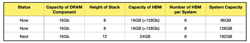
This varies by generation. The current HBM2E standard (an extension of second-generation HBM2) supports stacking of up to eight stacks, which would allow an HBM2E SiP to provide 128GB of capacity. In practice, however, currently available HBM2E capacities top out at 16GB. The HBM3 standard (now being developed) is expected to extend stacking capabilities — in conjunction with increasing device densities, this will produce significantly higher maximum capacities.
What advantage in bandwidth terms would HBM supply over DRAM?
This is where HBM’s advantages are most apparent in terms of bus width and processing speed. Since their first generation, HBM standards have supported a 1024-bit bus width, compared to just 32 bits for GDDR, and the standard HBM2E signaling rate is 3.6Gb per second (Gbit/sec) per pin, with up to 460GB per second (GB/sec) of bandwidth per stack. At this point in the development of HBM3, we expect to achieve the ever-fast processing speed of up to 6.4Gbit/sec — well above many expectations.
Unlike the case with capacity, however, in practice bandwidth has gone beyond the standard — Samsung’s HBM2E Flashbolt devices have a processing speed of 3.6Gbit/sec per pin, and bandwidth up to 460GB/sec. This compares to standard-specified data rates of 16Gbit/sec for the GDDR6 generation of DRAM. And for processors with a 4096-bit memory interface, such as GPUs and FPGAs, a combination of eight Flashbolt stacks can offer 128GB of memory with 3.68TB/sec peak bandwidth — far beyond traditional DRAM.
How would HBM be constructed in terms of, for example, number of stacks (layers) of DRAM and an interposer and a CPU?
As noted above, the current HBM2E standard supports up to eight dies each, while the as-yet-unreleased HBM3 standard is expected to increase the maximum number of dies.
Use of through-silicon vias and microbumps (rather than wire bonding) for interconnection of the stacked memory dies allows for a very small footprint and fast data transfer rates, while also enabling improved heat distribution to minimize thermal issues.
Moreover, use of a silicon interposer for interconnection of HBM stacks and processors means that the memory and processor can be in very close proximity for reduced access time, taking advantage of the high efficiency of silicon-based interconnections. The end result is both improved performance and substantially reduced energy consumption compared to the board-level interconnections typically used for traditional DRAM. And going forward, the interposer offers opportunities for inclusion of additional active circuitry that could advance the HBM model from its current 2.5D status to true 3D integration [including the very promising processor-in-memory [HBM-PIM] avenue].
Which supplier affixes the CPU to the HBM?
Assembly and test of the HBM and processor requires advanced techniques, but they are similar to those that are increasingly being used in chiplet-oriented designs where multiple dies are connected within an IC package. Each system OEM will make its own manufacturing supply chain decisions, but it seems now that members of the existing outsourced semiconductor assembly and test (OSAT) community (ASE, Amkor, etc.) will have the necessary capabilities as will some integrated device manufacturers (eg. Intel) and foundries (eg. TSMC).
Which CPUs would be supported? Which Xeon generation? Which AMD generation? Arm? Risc-V?
We are working with a variety of CPU developers. For ARM, Fujitsu is supplying and Xeon/RISC-V is currently developing.
Would/could HBM be connected to servers across a CXL bus? Is this a good or a bad idea?
We are deeply involved with the Compute Express Link (CXL) interconnect standard and continue to closely monitor its development. As with most technologies, the role of a specific memory technology will be determined in many ways by application requirements.
Will systems (servers, workstations, laptops) use both DRAM and HBM together? Why would they do this?
New products and projects have always presented system designers with unique sets of considerations on performance, power consumption, cost, form factor, time to market, and more. Today, with computing technology clearly in an era of unprecedented advancement, the calculations and tradeoffs are more complex than ever — with AI, ML, HPC and other emerging applications driving change at every level, from supercomputing centers to edge devices.
In response to these dynamics, and with traditional computing models and architectures under increasing pressure, engineering expectations for memories are rapidly evolving and diverging. As a result, an increasing array of memory types (GDDR6, HBM, DDR5, HBM+PIM, etc.) is now being used, especially in the HPC world, and this increasing heterogeneity is likely to extend to almost every market sector over time, as application demands grow more specialized. Again, these options are enablers for creative, innovative engineering and we expect designers to take advantage of all available options to meet their specific objectives.
Storage-class Memory (SCM)
What is happening with Z-NAND?
We are carefully reviewing the development direction of Z-NAND by collecting customer requirements.
If HBM is taken up by customers will there still be a need for SCM in the memory-storage hierarchy?
With the explosive growth in data generation, the need for delivering data-centric solutions for various workloads has never been greater. We are preparing solutions in close cooperation with a variety of partners to meet these radical demands for memory innovation.
What SCM technologies have attracted Samsung’s attention and why?
There are various workloads in the industry with different requirements, which should be addressed accordingly.
How does Samsung view Intel’s 3D XPoint technology?
As mentioned above, there are various needs in the industry, and a variety of solutions to address those needs.
Comment
Samsung is energetically active with DDR5 and DDR6 memory. It is also strongly developing its HBM and HBM-PIM stacked memory technology products. We note it’s thinking about HBM with X86, Arm and RISC-V processors. HBM-Arm and HBM-RISC-V would provide interesting competition for Xeon-HBM systems, particularly in edge environments with low-latency, data-intensive processing needs.
The Storage-class Memory situation is less clear-cut. It appears that Samsung sees a general need for SCM technology, but it’s possible application-specific technology may be needed rather than a single SCM technology.


