


NEO Semiconductor has patented X-NAND tech to accelerate SSD writes fifteenfold, and shrink die sizes. Two patents were awarded on August 5.
The company, founded by CEO Andy Hsu and Engineering VP Ray Tsay in 2016, won a Best of Show Award for Most Innovative Flash Memory Startup at the Flash Memory Summit 2020. It has devised a way to decrease page buffer capacity on a NAND die and parallelise operations, thereby increasing random and sequential read and write speeds as well.
Founder and CEO Andy Hsu issued a statement, saying: “Technological leaps have a history of driving innovation, so the expectations for NAND flash memory becoming faster by more than one order of magnitude are high. Imagine the possibilities when X-NAND QLC flash memory offers higher bandwidth than conventional SLC flash memory.”
SLC (1 bit/cell) flash is the fastest flash, and each additional bit in a cell means more voltage levels and slower read and write speeds plus lower endurance. X-NAND addresses the speed slowdown but not the endurance limitations of MLC (2 bits/cell), TLC (3 bits/cell), QLC (4 bits/cell) and PLC (5 bits/cell). Its main attribute is that it reduces a flash die’s page buffer size by 94 per cent.
This is said to enable the die plane count to be increased from two or four to 16 or more — up to 64. A plane is a collection of NAND cells that are read and written in a single operation, with different plane operations occurring in parallel. If sixteen IO operations can be carried out in parallel, rather than just two or four, then the die’s IO speed increases.
Neo claims its technology bumps up performance 27x for sequential reads, 15x for sequential writes, and 3x for random reads and writes. Neo claims its X-NAND architecture combines QLC density and SLC speed in 3D NAND flash memory, and stops SLC caches becoming completely full and thus inoperative. It also reduces the power needs of the die, enables its size to be reduced, and causes no increase in manufacturing cost. There is zero change to the NAND cell, array structure, process, and technology.
Closer look
A two-page white paper provides a short look at the technology, while a 16-page white paper provides a deeper dive.
The shorter doc explains: “X-NAND architecture allows one page buffer to perform read and write operations to 16 or more bit lines. This increases the number of planes in Y-direction to 16 times or more without increasing the number of total page buffers. As a result, the read and write data throughputs are increased by 16 times. In addition, because the bit line length and capacitance are reduced to 1/16, the random read speed and program-verification speed are drastically increased. The bit line power consumption is also reduced to 1/16.”
The 16-pager explains: “The program data is sequentially loaded to 16 bit lines by one page buffer, and held in the bit line capacitance to program 16 cells together. This significantly increases the write bandwidth of the page buffers. Because each program pulse is only 10μs, the data can be safely stored in the bit line capacitance without refresh operations.”
There is much, much more of interest to NAND die engineers and then a chart which should interest anyone interested in SSD performance:
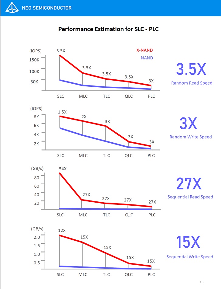
It’s a performance estimation, but just look at the numbers. First, sequential read and write operations are boosted more than random IO. Secondly, even SLC flash IO is accelerated, up to 54x — we specifically asked Neo to confirm this.
SLC speed and NAND endurance
A Neo spokesperson told us: “X-NAND SLC read and write speed can be increased. By using 16 planes (Y-direction), the random read/write speed can be increased by 2x/1.4x. The sequential read/write data throughput can be increased by 9x/5x time. By using 64 planes, the sequential read/write speed can be increased by 30x/22x. However, the above data is assuming the I/O speed can support that. In fact, X-NAND is so fast that the sequential speed will be limited by the I/O speed.”
We also asked if X-NAND could increase endurance. The spokesperson said: “By reducing the bit line length and capacitance, the read operation for X-NAND is more reliable than the conventional NAND which has very high bit line capacitance loading. This allows narrower and more accurately controlled Vt level for TLC to PLC; thus it is possible to improve the endurance cycles.”
The spokesperson added this point: “X-NAND has a feature called ‘SLC/(TLC-PLC) Parallel Programming’. This feature allows the data to be always written to SLC cells and then moved to TLC-PLC cells in parallel (simultaneously). X-NAND’s 16–64 plane architecture allows much more even ‘wear leveling’ than the conventional four planes. This will improve the endurance cycles.”
Neo notes
The company has ten employees and is funded by angel investors. The two US patents are number 11056190 B2 (Methods and apparatus for NAND flash memory) and number 11049579 B2.
It looks to us as if Neo will aim to license its technology to NAND manufacturers — meaning Kioxia, Intel, Micron, Samsung, SK hynix and Western Digital. That’s a small market in terms of companies.
Neo did win the Best of Show Award, and has been granted two patents for X-NAND, adding to its existing 20 or so patents. That means its technology is serious and worth a good look.


