


Tokyo Institute of Technology scientists have designed a 3D DRAM stack topped by a processor that they say can provide four times more bandwidth and one fifth of the bit access energy than High Bandwidth Memory (HBM)
HBM sidesteps the CPU-restricted socket count limitation on DRAM capacity by connecting small DRAM stacks to the CPU via an interposer layer. An individual DRAM die is connected to ones above or below by microbumps (connectors) with connecting holes (through-silicon vias or TSVs) passing through a die to connect microbumps, in a Bumpless Build Cube 3D (BBCube3D) concept.
Professor Takayuki Ohba, the research team lead, said: “The BBCube 3D has the potential to achieve a bandwidth of 1.6 terabytes per second, which is 30 times higher than DDR5 and four times higher than HBM2E.”
The researchers thinned each DRAM die and did away with the microbumps in their BBCube3D wafer-on-wafer (WOW) design. This can enable a memory block running at a higher speed and lower energy than either a DDR5 or an HBM2E (High Bandwith Memory gen 2 Extended) design as they run hotter and bumps add resistance/capacitance and delay.
HBM microbumps take up space and a die has to be stiff enough to withstand the pressure when the stack layers are bonded together. By eliminating them, each memory die can be made thinner and the TSVs shorter, which aids thermal cooling. There is no need for an interposer in the BBCube3D design as a processing unit, CPU or GPU, is bonded directly to a cache die which itself is bonded to the top of the DRAM stack.
The researchers say: “TSV interconnects with a short length provide the highest thermal dissipation from high-temperature devices such as CPUs and GPUs … high-density TSVs act as thermal pipes, and, hence, a low temperature, even in a 3D structure, can be expected.”
The BBCube “allows high bandwidth with low power consumption because of the short length of TSVs and high-density signal parallelism.”
Crosstalk in the layered DRAM was reduced by ensuring adjacent IO lines were out of phase with each other by adjusting their timings. This is called four-phase shielded inputs/outputs and means an IO line is never changing its value at the same time as its immediately neighboring lines.
Its speed and energy use were compared to those of DDR5 and HBM2E memory technologies. The chart shows a 32x bandwidth increase over DDR5 memory and a 4x speedup over HBM2E. At the same time the BBCube 3D design achieved a lower access energy rating than both DDR5 and HBM2E as well.
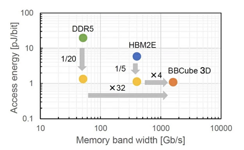
Ohba said: “Due to the BBCube’s low thermal resistance and low impedance, the thermal management and power supply issues typical of 3D integration can be relieved. As a result, the proposed technology could reach a remarkable bandwidth with a bit access energy that is 1/20th and 1/5th of DDR5 and HBM2E, respectively.”
This BBCube 3D is a university-level research project. A whole lot of detailed background information about the project can be found in an MDPI Electronics paper, “Review of Bumpless Build Cube (BBCube) Using Wafer-on-Wafer (WOW) and Chip-on-Wafer (COW) for Tera-Scale Three-Dimensional Integration (3DI). It says: “BBCube allowed stacking of 4-times more dies than HBM. This allowed the memory capacity to reach 64GB using 16Gb DRAM dies.”
It also said “terabit-capacity 3D memory can be realized by stacking 40 layers” of DRAM.
The BBCube 3D concept is described in a paper entitled “Bumpless Build Cube (BBCube) 3D: Heterogeneous 3D Integration Using WoW and CoW to Provide TB/s Bandwidth with Lowest Bit Access Energy” presented at a June 2023 IEEE 2023 Symposium on VLSI Technology and Circuits.


