


Samsung has demonstrated an in-memory computing MRAM chip processing stored data, and accurately working on AI problems such as face detection. A Nature paper is coming to explain how it was done
This technology could provide low-power dedicated AI chips combining compute and storage to reduce data movement, speed processing and lower energy use. It could also help develop neuromorphic computing — analogous to how masses of neurons and synapses in the brain inter-operate.
Lead paper author Dr Seungchul Jung is quoted in Samsung’s announcement: “In-memory computing draws similarity to the brain in the sense that in the brain, computing also occurs within the network of biological memories, or synapses, the points where neurons touch one another.
“In fact, while the computing performed by our MRAM network for now has a different purpose from the computing performed by the brain, such solid-state memory network may in the future be used as a platform to mimic the brain by modelling the brain’s synapse connectivity.”
MRAM technology
MRAM or magneto-resistive RAM, also known as spin-transfer torque magneto-resistive RAM (STT-MRAM), relies on the different spin directions of electrons to signal a binary one or zero.
It is a non-volatile memory technology with greater speed and endurance than NAND. While it has been actively investigated as a possibility for replacing SRAM for many years, progress has been limited as it is a difficult technology to develop, with high manufacturing costs.
As we wrote back in 2018, STT-MRAM cells or storage elements have two ferromagnetic plates, electrodes, separated by non-magnetic material. One high-coercivity electrode has its magnetism pinned because it needs a larger magnet field or spin-polarised current to change its magnetic orientation compared to the other electrode.
This second, lower coercivity electrode is called a free layer and its north-south orientation can be changed more easily. Binary values are stored by making the free electrode have the same, parallel, north-south orientation as the reference electrode or a different, anti-parallel one. The electrical resistance of the cell, due to the spin-polarised electron tunnelling effect, is different in each state, indicating a binary value.
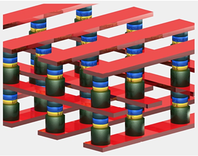
The complexity of the technology can be seen in developer Spin Memory’s product, using a 3D two-level cell crossbar array — it involves more than 250 separate patents.
Everspin is another MRAM developer and its STT-MRAM offers higher write and read speeds than DRAM and has been used by IBM in its FlashSystem 9100 and Storwise V7000 systems. In effect, MRAM is in commercial production already but it is a niche technology.
Compute this
Samsung’s neat idea is to use MRAM differently, by adding compute elements to an MRAM chip built as a 64×64 cell crossbar array, and use its data access speed and non-volatility along with in-chip parallel processing to speed AI tasks. Naturally the scope of the compute is limited — you can’t realistically add general-purpose CPU cores to blocks of cells in a memory chip, but you can add small processors with limited instruction sets.
Samsung has been working on processing-in-memory (PIM) ideas for some time. For example, it has an Aquabolt-XL HBM2 chip embedding a programmable computing unit (PCU) inside each memory bank, minimising the need for data movement.
Samsung MRAM tack
The Samsung MRAM researchers took a different tack. They thought that the low resistance of MRAM cells meant that MRAM PIM chips would need more power than computing ReRAM and Phased Change Memory (PCM) technologies. But if they changed the MRAM chip design or architecture from what is called “current-sum” to an alternative “resistance sum” for analogue multiply–accumulate operations, which they say addresses the problem of small resistances of individual MRAM devices.
Analogue AI PIM technology promises to use much less electrical power than computing artificial neural networks (ANNs) in digital processors.
We’d like to understand this much more but the details are hidden behind scientific paper paywalls. The paper’s available diagrams talk about Artificial Neural Networks and performing analogue vector–matrix multiplication to transfer data from a layer to the next. The paper abstract mentions “multiply–accumulate operations prevalent in artificial neural networks.“
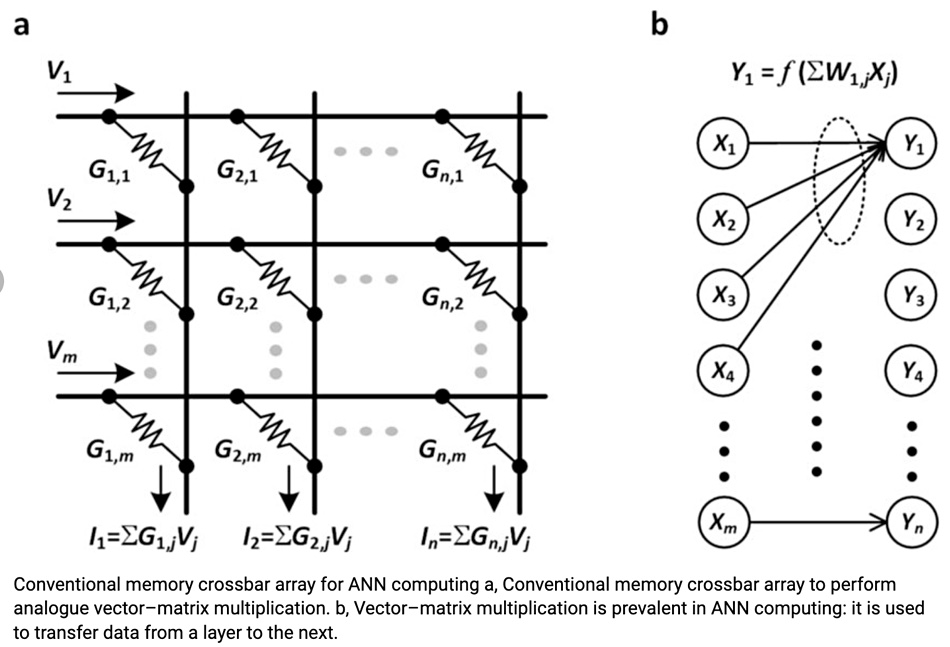
We have found a preliminary copy, and its first page compares in-memory processing and conventional Von Neuman architecture. “The rate at which data can be transferred between the processing unit and the memory unit represents a fundamental limitation of modern computers, known as the memory wall. In-memory computing is an approach that attempts to address this issue by designing systems that compute within the memory, thus eliminating the energy-intensive and time-consuming data movement that plagues current designs.”
The researchers’ MRAM crossbar array design is explained like this: “With each memory storing a synaptic weight as its conductance value, the crossbar array executes the vector–matrix multiplication, the most prevalent ANN algebra. Each column yields a dot product between the input voltage vector fed to the rows and the column weight vector, by first multiplying the memory conductance and the input voltage at each row–column cross-point via Ohm’s law and subsequently summing the resulting cross-point currents along the column via Kirchhoff’s law.
“This physical matrix multiplication, or analogue multiply–accumulate (MAC) operation, consumes far less power than its digital counterpart.”
Once the researchers had the designed chip available they tested it on a couple of classic AI problems. It achieved an accuracy of 98 per cent in classification of hand-written digits and a 93 per cent accuracy in detecting faces from scenes.
Comment
This compute-in memory MRAM chip looks highly specialised for specific types of AI problems and is unlikely to appear in enterprise computing until it needs to deal with such problems in a routine way.
Bootnote: The paper, “A crossbar array of magnetoresistive memory devices for in-memory computing”, has been published online by Nature and paper-based publication is coming shortly.
The research was led by Samsung Advanced Institute of Technology (SAIT) in collaboration with Samsung Electronics Foundry Business and Semiconductor R&D Center. The first author of the paper, Dr Seungchul Jung, staff researcher at SAIT, and the co-corresponding authors Dr Donhee Ham, fellow of SAIT and professor of Harvard University, and Dr Sang Joon Kim, vice president of technology at SAIT, led the research.


