


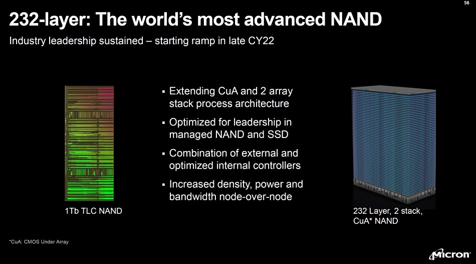
Micron spoke of 232-layer SSD tech and a “combination of external and optimized internal controllers” at its recent Investor Day Conference.
This was picked up by Jim “The SSD Guy” Handy, who heard technology and product veep Scott DeBoer say that Micron makes vertically integrated SSDs which include NAND, some DRAM, and the controller. DeBoer said Micron is using an in-house controller because a portion of it was incorporated into the NAND flash chips themselves.
The controller was split between external and internal functions. Why? It means some NAND controller functions can be performed by the NAND chips inside an SSD – low-level functions internal to a chip. That means they could occur in parallel, offload the SSD controller so it can do other work, and enable the SSD to work faster overall.
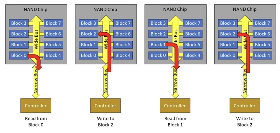
Handy said an SSD typically has a controller inside it – Micron’s “external controller” phrase – which links to NAND chips across a relatively narrow bus. Each NAND chip is subdivided into blocks and these are linked by a wide internal bus, which is connected to the narrow bus going to/from the controller.
In a process such as the recovery of partially erased blocks – garbage collection – valid data is read from blocks needing to be recovered and copied to an empty block. When all the data from partially erased blocks has been read into the new block, the old blocks’ contents are deleted and they become empty blocks available for reuse. Handy has a diagram showing this:
Such garbage collection is directed by the controller, which reads then writes the data involved in the process. While it is carried out, this internal-to-the-SSD process it is not available to perform its main work, reading and writing data to/from the SSD for its host server or single-user system.
Handy suggests that this could be done by putting appropriate internal controller functions – simple ones – inside the NAND chips. For example, the external controller would decide that garbage collection was needed and, using its metadata map of NAND empty and used chip blocks and data contents, calculate a series of block data reads and writes and subsequent block deletions as before. Then it would tell the NAND chips to do the work themselves, and eliminate the internal SSD IO of data reads and writes to/from the controller. A second Handy diagram illustrates the concept:
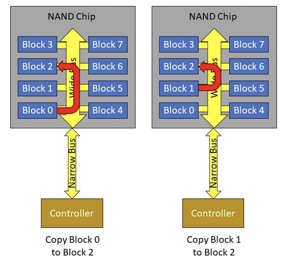
The controller, for example, tells a NAND chip internal controller function to read valid data from block 0 to block 2, then valid data from block 1 to block 2, then delete block 0 and block 1. The data is transferred across the NAND chip’s wide bus, hence it is faster, and the external controller is not directly involved in the IO at all.
What we have here looks like a potential variant of the processing-in-memory (PIM) idea (think Samsung’s Aquabolt AI processor). We could call it PIN – processing-in-NAND. It is literally compute in storage, albeit very simple compute.
This, Handy says, is only a possibility. He writes: “Micron may be doing something altogether different. The company’s engineers may have chosen more appropriate functions to pull into the NAND. In the end, though, the new NAND functions, whatever they are, probably accelerate the SSD while reducing the controller’s complexity and cost. I would also assume that Micron plans to keep these functions confidential, so that only Micron SSDs can take advantage of them. This would give the company a distinct competitive edge.”
It seems a powerful idea and Handy suggests we should “expect to see this approach adopted by other NAND flash makers in the future.”
We must wait and see what Micron announces as it brings out 233-layer 3D NAND SSDs. The signs we’ll be looking for include better-than-expected SSD performance.


