UK university research spin-out Intrinsic Semiconductor Technology’s ReRAM can be made on the same CMOS wafers as microcontrollers, enabling them to have embedded SRAM-speed non-volatile memory with no need for external NAND chips.
Intrinsic was founded in 2017 by two University College of London (UCL) researchers: Professor Anthony Kenyon and Dr Adnan Mehonic. Their research into Silicon Oxide (SiOx)-based memristors led them to a technology using conductive filaments composed of oxygen vacancies. The amount of oxygen in the filament can be varied to determine the resistance of the SiOx material – high or low.
Professor Tony Kenyon, co-founder and CTO of Intrinsic, and Professor of Nanoelectronic & Nanophotonic Materials at UCL, said “Existing memory technologies, such as Flash, are reaching the limits of their capabilities – particularly in embedded systems such as those we need in IoT devices. Intrinsic’s memristor technology will transform next generation systems by combining high performance with ease of integration in digital CMOS. By basing our devices on silicon oxide, we ensure that they are as simple and as cheap to integrate with silicon-based electronics as it is possible to be.”
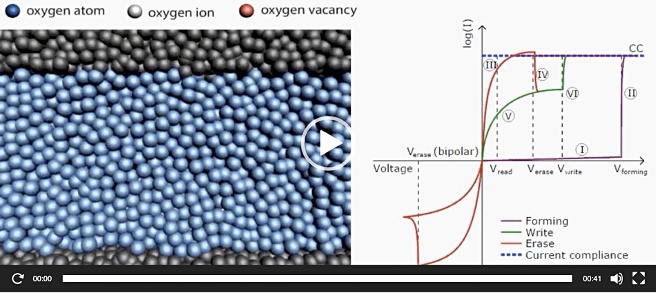
Oxygen ions are forced in to the filament or removed by set/reset electrical currents, and the end state is stable at 270℃ and higher – more than adequate for solder reflow temperatures. An Intrinsic video schematically shows the oxygen ion movement along with set/reset and read voltage charts:

Intrinsic says its oxygen vacancy ReRAM is faster, lower cost and uses less energy than NAND. It will deliver its first products as embedded non-volatile memories for integration into CMOS digital logic devices using standard EDA design flows.

Dr Mark Dickinson was appointed CEO in April 2019. He was previously an EVP at Imagination Technologies and a VP at Arm.
Intrinsic received £1.35 million ($1.8 million) in seed funding in March 2021 from the UCL Technology Fund and IP Group. This enabled it to partner with imec, a Belgian semiconductor research and development operation based in Leuven, to transfer Intrinsic’s technology to a standard CMOS process on 300mm wafers.
This partnership has demonstrated the scaling of Intrinsic’s ReRAM to 50nm, and the necessary switching behaviour and electrical performance needed for its operation as embedded non-volatile memory in microcontroller chips used in edge AI and IoT applications.
Dickinson said in a funding round statement: “Having seen the potential for new memory technologies to disrupt the sector in my time in senior roles at Arm and Imagination, I am excited to be working with two of the most prominent researchers in the field to bring the best memristor technology to market. This is an exciting invention from a leading UK university with the potential for truly global impact.”
A statement from Mehonic mentioned more applications. “The overall performance of hardware we use for AI is determined and limited by the bandwidth and energy-efficiency of memory technologies. A fast, energy-efficient, cheap and scalable non-volatile memory that can be incorporated directly on a chip, such as our silicon oxide memristors, will significantly improve the performance, especially for energy-efficient edge computing. Furthermore, our technology could be utilised for analogue AI hardware accelerators currently in development and novel computing paradigms, such as neuromorphic and spiking-based computing.”
The key Intrinsic pitch is that any chip designer will be able to embed its ReRAM non-volatile memory on the chip, with the ReRAM as fast to read as SRAM (static random access memory ), but at a fraction of the cost and power consumption. And, of course, the ReRAM is non-volatile whilst the SRAM is not. We don’t have actual read and write times but understand the read time is less than 100 nanoseconds.
Dickinson said “It is the simplicity of our device that really makes it stand out from other emerging memories. We use materials and processes that are commonplace in CMOS manufacturing to create these exceptional memory devices. Our mission is to make a fast and low-cost, embedded, non-volatile memory available to any chip architect who wants to use it. In particular, applications such as edge AI or IoT, where low power consumption and high performance are key, can move from using an expensive and power-hungry external memory to a fully integrated single-chip architecture.”
Comment
Weebit Nano is another startup developing ReRAM. Its technology also uses oxygen filament formation in silicon oxide material. Like Intrinsic it is working with an external research agency: CEA/Leti in France.
Like Intrinsic again it claims its ReRAM materials are CMOS-friendly and can be easily and cost-effectively added to the final stages of a semi-conductor process – BEOL or back end of line – with a two-mask adder and five to eight per cent extra wafer cost. Weebit and CEA-Lei have demonstrated an operational ReRAM crossbar array and the technology has been scaled down to 28nm.


