


University of Lancaster researchers have devised a universal memory candidate technology.
By using a structure based on members of the III-V chemical compounds family, it’s possible to build a memory cell with the switching speed of DRAM, data retention that’s better than NAND, and a far lower voltage needed for switching than NAND.
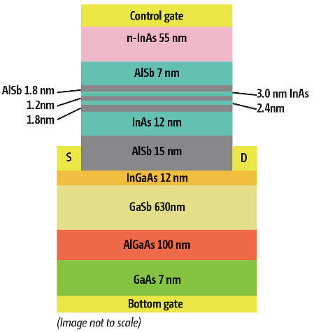
It is called an UltraRAM cell and uses an Indium arsenide (InAs) floating gate to store the memory state (bit value). This gate is isolated by a layered barrier built from Indium arsenide and Aluminium antimonide as this diagram illustrates;
A schematic diagram expands on this;
Interactions between the layers traps the memory state charge in the floating gate. The isolation of the floating gate is such that the cell holds data for an extremely long time. In fact a retention period of an extraordinary 100 trillion years has been predicted through a simulation exercise.
The cell’s state can be altered by a slightly larger than 2 volt current, taking advantage of a dual quantum well resonant tunnelling junction through the isolating barrier. This is said by the researchers to be 0.1 per cent of the energy needed to switch NAND and 1 per cent of that needed to switch DRAM.
Writing logic state 1, adding charge, takes just over 5ns, while writing logic state 0, emptying charge, takes 3ns.
The UltraRAM cell is described in pay-to-download paper; Simulations of Ultralow-Power Nonvolatile Cells for Random-Access Memory. But the initial research is in a free-to-download report; Room-temperature Operation of Low-voltage, Non-volatile, Compound-semiconductor Memory Cells.
These papers have been authored by Professor Manus Hayne and PhD student Dominic Lane, both in the university’s Physics research facility.
They say the cells can be built into bit-addressable arrays and so used for computing stage /memory devices. Watch this space to see if the research technology can be productised.
II-V Compounds
The III-V compounds or alloys are composed of particular elements in the table of elements, in the boron (III) and orogen (V) groups. The ones used by the researchers are:
- InGaAs – Indium gallium arsenide – a room-temperature semiconductor,
- GaSb – Gallium antimonide – a semiconducting compound,
- AlGaAs – Aluminium gallium arsenide – a non-conductor and used as a barrier material in GaAs-based heterostructure devices,
- GaAs – Gallium arsenide – a compound semiconductor,
- AlSb – Aluminium antimonide – another compound semiconductor,
- InAs – Indium arsenide – another semiconductor.


